
Your Feedback is Important to Us!
Please take a moment to participate in our short survey.
At onsemi, we are dedicated to delivering technical content that best
meets your needs.
Help Us Improve – Take the Survey
This survey is intended to collect your feedback, capture any issues you may
encounter, and to provide improvements you would like to suggest.
We look forward to your feedback.
To learn more about onsemi, please visit our website at
www.onsemi.com
Thank you for your interest in onsemi products.
Your technical document begins on the following pages.
onsemi and and other names, marks, and brands are registered and/or common law trademarks of Semiconductor Components Industries, LLC dba “onsemi” or its affiliates and/or
subsidiaries in the United States and/or other countries. onsemi owns the rights to a number of patents, trademarks, copyrights, trade secrets, and other intellectual property. A listing of onsemi
product/patent coverage may be accessed at www.onsemi.com/site/pdf/Patent-Marking.pdf. onsemi reserves the right to make changes at any time to any products or information herein, without
notice. The information herein is provided “as-is” and onsemi makes no warranty, representation or guarantee regarding the accuracy of the information, product features, availability, functionality,
or suitability of its products for any particular purpose, nor does onsemi assume any liability arising out of the application or use of any product or circuit, and specifically disclaims any and all
liability, including without limitation special, consequential or incidental damages. Buyer is responsible for its products and applications using onsemi products, including compliance with all laws,
regulations and safety requirements or standards, regardless of any support or applications information provided by onsemi. “Typical” parameters which may be provided in onsemi data sheets and/
or specifications can and do vary in different applications and actual performance may vary over time. All operating parameters, including “Typicals” must be validated for each customer application
by customer’s technical experts. onsemi does not convey any license under any of its intellectual property rights nor the rights of others. onsemi products are not designed, intended, or authorized
for use as a critical component in life support systems or any FDA Class 3 medical devices or medical devices with a same or similar classification in a foreign jurisdiction or any devices intended for
implantation in the human body. Should Buyer purchase or use onsemi products for any such unintended or unauthorized application, Buyer shall indemnify and hold onsemi and its officers, employees,
subsidiaries, affiliates, and distributors harmless against all claims, costs, damages, and expenses, and reasonable attorney fees arising out of, directly or indirectly, any claim of personal injury or death
associated with such unintended or unauthorized use, even if such claim alleges that onsemi was negligent regarding the design or manufacture of the part. onsemi is an Equal Opportunity/Affirmative
Action Employer. This literature is subject to all applicable copyright laws and is not for resale in any manner. Other names and brands may be claimed as the property of others.

DATA SHEET
www.onsemi.com
© Semiconductor Components Industries, LLC, 2016
August, 2021 − Rev. 6
1 Publication Order Number:
NOIP1SN1300A/D
PYTHON 1.3/0.5/0.3 MegaPixels
Global Shutter CMOS
Image Sensors
NOIP1SN1300A
FEATURES
• Size Options:
♦ PYTHON 300: 640 x 480 Active Pixels, 1/4” Optical Format
♦ PYTHON 500: 800 x 600 Active Pixels, 1/3.6” Optical Format
♦ PYTHON 1300: 1280 x 1024 Active Pixels, 1/2” Optical Format
• Data Output Options:
♦ P1−SN/SE/FN: 4 LVDS Data Channels
♦ P2−SN/SE: 10 bit Parallel
♦ P3−SN/SE/FN: 2 LVDS Data Channels
• 4.8 mm x 4.8 mm Low Noise Global Shutter Pixels with
In-pixel CDS
• Monochrome (SN), Color (SE) and NIR (FN)
• Zero Row Overhead Time (ZROT) Mode Enabling
Higher Frame Rate
• Frame Rate at Full Resolution, 4 LVDS Data Channels
(P1−SN/SE/FN only)
♦ 210/165 frames per second @ SXGA
(ZROT/NROT)
♦ 545/385 frames per second @ SVGA
(ZROT/NROT)
♦ 815/545 frames per second @ VGA (ZROT/NROT)
• Frames Rate at Full Resolution (CMOS)
♦ 50/43 Frames per Second @ SXGA (ZROT/NROT)
• On−chip 10−bit Analog−to−Digital Converter (ADC)
• Four/Two/One LVDS High Speed Serial Outputs or
Parallel CMOS Output
• Random Programmable Region of Interest (ROI)
Readout
• Serial Peripheral Interface (SPI)
• Automatic Exposure Control (AEC)
• Phase Locked Loop (PLL)
• High Dynamic Range (HDR) Modes Possible
• Dual Power Supply (3.3 V and 1.8 V)
• −40°C to +85°C Operational Temperature Range
• 48−pin LCC
• Power Dissipation:
♦ 620 mW (P1, 4 LVDS, ZROT)
♦ 420 mW (P1, P3, 2 LVDS, NROT)
♦ 270 mW (P1, P3, 1 LVDS, NROT)
♦ 420 mW (P2, ZROT)
• These Devices are Pb−Free and are RoHS Compliant
APPLICATIONS
• Machine Vision
• Motion Monitoring
• Security
• Barcode Scanning (2D)
DESCRIPTION
The PYTHON 300, PYTHON 500, and PYTHON 1300
image sensors utilize high sensitivity 4.8 mm x 4.8 mm pixels
that support low noise “pipelined” and “triggered” global
shutter readout modes. The sensors support correlated
double sampling (CDS) readout, reducing noise and
increasing dynamic range.
The image sensors have on−chip programmable gain
amplifiers and 10−bit A/D converters. The integration time
and gain parameters can be reconfigured without any visible
image artifact. Optionally the on−chip automatic exposure
control loop (AEC) controls these parameters dynamically.
The image’s black level is either calibrated automatically or
can be adjusted by adding a user programmable offset.
A high level of programmability using a four wire serial
peripheral interface enables the user to read out specific
regions of interest. Up to eight regions can be programmed,
achieving even higher frame rates.
The image data interface of the P1−SN/SE/FN devices
consists of four LVDS lanes, enabling frame rates up to 210
frames per second in Zero ROT mode for the
PYTHON 1300. Each channel runs at 720 Mbps. A separate
synchronization channel containing payload information is
provided to facilitate the image reconstruction at the
receiving end. The P2−SN/SE devices provide a parallel
CMOS output interface at reduced frame rate. The
P3−SN/SE/FN devices are the same as the P1−SN/SE/FN
but with only two of the four LVDS data channels enabled,
facilitating frame rates of 90 frames per second in Normal
ROT for the PYTHON 1300.
Figure 1. PYTHON 1300

NOIP1SN1300A
www.onsemi.com
2
The devices are provided in a 48−pin LCC package and are available in monochrome, Bayer color, and extended
near−infrared (NIR) configurations.
ORDERING INFORMATION
Part Number Description Package
PYTHON 1300
NOIP1SN1300A−QDI
1.3 Megapixel, Monochrome, LVDS Output
48−pin LCC
NOIP1SE1300A−QDI 1.3 Megapixel, Bayer Color, LVDS Output
NOIP1FN1300A−QDI 1.3 Megapixel, Monochrome with enhanced NIR, LVDS Output
NOIP2SN1300A−QDI 1.3 Megapixel, Monochrome, CMOS (parallel) Output
NOIP2SE1300A−QDI 1.3 Megapixel, Bayer Color, CMOS (parallel) Output
NOIP1SN1300A−QTI 1.3 Megapixel, Monochrome, LVDS Output, Protective Foil
NOIP1SE1300A−QTI 1.3 Megapixel, Bayer Color, LVDS Output, Protective Foil
NOIP1FN1300A−QTI 1.3 Megapixel, Monochrome with enhanced NIR, LVDS Output, Protective Foil
NOIP3SN1300A−QDI 1.3 Megapixel, 2 LVDS Outputs, Monochrome
NOIP3FN1300A−QDI 1.3 Megapixel, 2 LVDS Outputs, NIR enhanced Monochrome
NOIP3SE1300A−QDI 1.3 Megapixel, 2 LVDS Outputs, Color
NOIP3SN1300A−QTI 1.3 Megapixel, 2 LVDS Outputs, Monochrome, Protective Foil
NOIP3FN1300A−QTI 1.3 Megapixel, 2 LVDS Outputs, NIR enhanced Monochrome, Protective Foil
NOIP3SE1300A−QTI 1.3 Megapixel, 2 LVDS Outputs, Color, Protective Foil
PYTHON 500
NOIP1SN0500A−QDI
0.5 Megapixel, Monochrome, LVDS Output
48−pin LCC
NOIP1SE0500A−QDI 0.5 Megapixel, Bayer Color, LVDS Output
NOIP1FN0500A−QDI 0.5 Megapixel, Monochrome with enhanced NIR, LVDS Output
NOIP1SN0500A−QTI 0.5 Megapixel, Monochrome, LVDS Output, Protective Foil
NOIP1SE0500A−QTI 0.5 Megapixel, Bayer Color, LVDS Output, Protective Foil
NOIP1FN0500A−QTI 0.5 Megapixel, Monochrome with enhanced NIR, LVDS Output, Protective Foil
PYTHON 300
NOIP1SN0300A−QDI
0.3 Megapixel, Monochrome, LVDS Output
48−pin LCC
NOIP1SE0300A−QDI 0.3 Megapixel, Bayer Color, LVDS Output
NOIP1FN0300A−QDI 0.3 Megapixel, Monochrome with enhanced NIR, LVDS Output
NOIP1SN0300A−QTI 0.3 Megapixel, Monochrome, LVDS Output, Protective Foil
NOIP1SE0300A−QTI 0.3 Megapixel, Bayer Color, LVDS Output, Protective Foil
NOIP1FN0300A−QTI 0.3 Megapixel, Monochrome with enhanced NIR, LVDS Output, Protective Foil
The P1−SN/SE/FN base part references the mono, color and NIR enhanced versions of the 4 LVDS interface; the P2−SN/SE
base part references the mono and color versions of the CMOS interface; the P3−SN/SE/FN base part references the mono,
color and NIR enhanced version of the 2 LVDS interface. More details on the part number coding can be found at
http://www.onsemi.com/pub_link/Collateral/TND310−D.PDF
Production Package Mark
Line 1: NOIPyxxRRRRA where y is either “1” for 4 LVDS Outputs, “2” for CMOS Parallel Output, “3” for 2 LVDS Outputs,
where xx denotes mono micro lens (SN) or color micro lens (SE) or NIR micro lens (FN)
RRRR is the resolution (1300), (0500) or (0300)
Line 2: −QDI (without protective foil), −QTI (with protective foil)
Line 3: AWLYYWW where AWL is PRODUCTION lot traceability, YYWW is the 4−digit date code

NOIP1SN1300A
www.onsemi.com
3
SPECIFICATIONS
Key Specifications
Table 1. GENERAL SPECIFICATIONS
Parameter Specification
Pixel type In−pixel CDS. Global shutter pixel
architecture
Shutter type Pipelined and triggered global shutter
Frame rate
Zero ROT/
Normal ROT
mode
P1−SN/SE/FN:
PYTHON 300: 815/545 fps
PYTHON 500: 545/385 fps
PYTHON 1300: 210/165 fps
P2−SN/SE: 50/43 fps
P3−SN/SE/FN: NA/90 fps
Master clock P1, P3−SN/SE/FN:
72 MHz when PLL is used,
360 MHz (10−bit) / 288 MHz (8−bit)
when PLL is not used
P2−SN/SE: 72 MHz
Windowing 8 Randomly programmable windows. Nor-
mal, sub−sampled and binned readout
modes
ADC resolution 10−bit, 8−bit (Note 1)
LVDS outputs P1−SN/SE/FN: 4/2/1 data + sync + clock
P3−SN/SE/FN: 2/1 data + sync + clock
CMOS outputs P2−SN/SE: 10−bit parallel output,
frame_valid, line_valid, clock
Data rate P1−SN/SE/FN:
4 x 720 Mbps (10−bit) /
4 x 576 Mbps (8−bit)
P2−SN/SE: 72 Mhz
P3−SN/SE/FN: 2 x 720 Mbps (10−bit)
Power
dissipation
(10−bit mode)
P1−SN/SE/FN: 620 mW (4 data channels)
P1, P3−SN/SE/FN: 420 mW (2 data ch.)
P1, P3−SN/SE/FN: 270 mW (1 data ch.)
P2−SN/SE: 420 mW
Package type 48−pin LCC
Table 2. ELECTRO−OPTICAL SPECIFICATIONS
Parameter Specification
Active pixels PYTHON 300: 640 (H) x 480 (V)
PYTHON 500: 800 (H) x 600 (V)
PYTHON 1300: 1280 (H) x 1024 (V)
Pixel size
4.8 mm x 4.8 mm
Conversion gain 0.096 LSB10/e
−
140 mV/e
−
Dark temporal noise < 9 e
−
(Normal ROT, 1x gain)
< 7 e
−
(Normal ROT, 2x gain)
Responsivity
at 550 nm
7.7 V/lux.s
Parasitic Light
Sensitivity (PLS)
<1/8000
Full Well Charge 10000 e
−
Quantum Efficiency
at 550 nm
56%
Pixel FPN < 1.0 LSB10
PRNU < 2% or 10 LSB10 on half scale
response of 525LSB10
MTF 68% @ 535 nm − X−dir & Y−dir
PSNL at 20°C 120 LSB10/s, 1200 e
−
/s
Dark signal at 20°C 5 e
−
/s, 0.5 LSB10/s
Dynamic Range > 60 dB in global shutter mode
Signal to Noise Ratio
(SNR max)
40 dB
Table 3. RECOMMENDED OPERATING RATINGS (Note 2)
Symbol
Description Min Max Unit
T
J
Operating temperature range −40 85 °C
Functional operation above the stresses listed in the Recommended Operating Ranges is not implied. Extended exposure to stresses beyond
the Recommended Operating Ranges limits may affect device reliability.
Table 4. ABSOLUTE MAXIMUM RATINGS (Notes 3 and 4)
Symbol
Parameter Min Max Unit
ABS (1.8 V supply group) ABS rating for 1.8 V supply group –0.5 2.2 V
ABS (3.3 V supply group) ABS rating for 3.3 V supply group –0.5 4.3 V
T
S
ABS storage temperature range −40 +150 °C
ABS storage humidity range at 85°C 85 %RH
Electrostatic discharge (ESD)
Human Body Model (HBM): JS−001−2010 2000
V
Charged Device Model (CDM): JESD22−C101 500
LU Latch−up: JESD−78 100 mA
Stresses exceeding those listed in the Maximum Ratings table may damage the device. If any of these limits are exceeded, device functionality
should not be assumed, damage may occur and reliability may be affected.
1. The ADC is 11−bit, down−scaled to 10−bit. The PYTHON uses a larger word−length internally to provide 10−bit on the output.
2. Operating ratings are conditions in which operation of the device is intended to be functional.
3. onsemi recommends that customers become familiar with, and follow the procedures in JEDEC Standard JESD625−A. Refer to Application
Note AN52561. Long term exposure toward the maximum storage temperature will accelerate color filter degradation.
4. Caution needs to be taken to avoid dried stains on the underside of the glass due to condensation. The glass lid glue is permeable and can
absorb moisture if the sensor is placed in a high % RH environment.

NOIP1SN1300A
www.onsemi.com
4
Table 5. ELECTRICAL SPECIFICATIONS
Boldface limits apply for T
J
= T
MIN
to T
MAX
, all other limits T
J
= +30°C. (Notes 5, 6, 7, 8 and 9)
Parameter
Description Min Typ Max Unit
Power Supply Parameters − P1 − SN/SE/FN LVDS (ZROT)
(NOTE: All ground pins (gnd_18, gnd_33, gnd_colpc) should be connected to an external 0 V ground reference.)
vdd_33
Supply voltage, 3.3 V 3.2 3.3 3.4 V
Idd_33 Current consumption 3.3 V supply 140 mA
vdd_18 Supply voltage, 1.8 V 1.7 1.8 1.9 V
Idd_18 Current consumption 1.8 V supply 80 mA
vdd_pix Supply voltage, pixel 3.25 3.3 3.35 V
Idd_pix Current consumption pixel supply 5 mA
Ptot Total power consumption at vdd_33 = 3.3 V, vdd_18 = 1.8 V
P1−SN/SE/FN, 4 LVDS, ZROT
620 mW
Pstby_lp Power consumption in low power standby mode 50 mW
Popt Power consumption at lower pixel rates Configurable
Power Supply Parameters − P3 − SN/SE/FN LVDS (NROT)
(NOTE: All ground pins (gnd_18, gnd_33, gnd_colpc) should be connected to an external 0 V ground reference.)
vdd_33
Supply voltage, 3.3 V 3.2 3.3 3.4 V
Idd_33 Current consumption 3.3 V supply (2 / 1 LVDS) 95 / 55 mA
vdd_18 Supply voltage, 1.8 V 1.7 1.8 1.9 V
Idd_18 Current consumption 1.8 V supply (2 / 1 LVDS) 55 / 45 mA
vdd_pix Supply voltage, pixel 3.25 3.3 3.35 V
Idd_pix Current consumption pixel supply (2 / 1 LVDS) 2 / 1 mA
Ptot Total power consumption at vdd_33 = 3.3 V, vdd_18 = 1.8 V
P3−SN/SE/FN, 2 LVDS, NROT
P3−SN/SE/FN, 1 LVDS, NROT
420
270
mW
Pstby_lp Power consumption in low power standby mode 50 mW
Popt Power consumption at lower pixel rates Configurable
Power Supply Parameters − P2−SN/SE CMOS
vdd_33
Supply voltage, 3.3 V 3.2 3.3 3.4 V
Idd_33 Current consumption 3.3 V supply 120 mA
vdd_18 Supply voltage, 1.8 V 1.7 1.8 1.9 V
Idd_18 Current consumption 1.8 V supply 10 mA
vdd_pix Supply voltage, pixel 3.25 3.3 3.35 V
Idd_pix Current consumption pixel supply 1 mA
Ptot Total power consumption 420 mW
Pstby_lp Power consumption in low power standby mode 50 mW
Popt Power consumption at lower pixel rates Configurable
I/O − P1−SN/SE/FN, P3−SN/SE/FN LVDS (EIA/TIA−644): Conforming to standard/additional specifications and deviations listed
fserdata
Data rate on data channels
DDR signaling − 4 data channels, 1 synchronization channel
720 Mbps
Product parametric performance is indicated in the Electrical Characteristics for the listed test conditions, unless otherwise noted. Product
performance may not be indicated by the Electrical Characteristics if operated under different conditions.
5. All parameters are characterized for DC conditions after thermal equilibrium is established.
6. This device contains circuitry to protect the inputs against damage due to high static voltages or electric fields. However, it is
recommended that normal precautions be taken to avoid application of any voltages higher than the maximum rated voltages to this high
impedance circuit.
7. Minimum and maximum limits are guaranteed through test and design.
8. Refer to ACSPYTHON1300 available at the Image Sensor Portal for detailed acceptance criteria specifications.
9. For power supply management recommendations, please refer to Application Note AND9158.

NOIP1SN1300A
www.onsemi.com
5
Table 5. ELECTRICAL SPECIFICATIONS
Boldface limits apply for T
J
= T
MIN
to T
MAX
, all other limits T
J
= +30°C. (Notes 5, 6, 7, 8 and 9)
Parameter UnitMaxTypMinDescription
fserclock Clock rate of output clock
Clock output for mesochronous signaling
360 MHz
Vicm LVDS input common mode level 0.3 1.25 1.8 V
Tccsk Channel to channel skew (Training pattern allows per channel
skew correction)
50 ps
I/O − P2−SN/SE CMOS (JEDEC− JESD8C−01): Conforming to standard/additional specifications and deviations listed
fpardata
Data rate on parallel channels (10−bit) 72 Mbps
Cout Output load (only capacitive load) 10 pF
tr Rise time (10% to 90% of input signal) 2.5 4.5 6.5 ns
tf Fall time (10% to 90% of input signal) 2 3.5 5 ns
Electrical Interface − P1 − SN/SE/FN LVDS
fin
Input clock rate when PLL used 72 MHz
fin Input clock when LVDS input used 360 MHz
tidc Input clock duty cycle when PLL used 45 50 55 %
tj Input clock jitter 20 ps
ratspi
(= fin/fspi)
10−bit (4 LVDS channels), PLL used 6
10−bit (2 LVDS channels), PLL used 12
10−bit (1 LVDS channel), PLL used 24
10−bit (4 LVDS channels), LVDS input used 30
10−bit (2 LVDS channels), LVDS input used 60
10−bit (1 LVDS channel), LVDS input used 120
8−bit (4 LVDS channels), PLL used 6
8−bit (2 LVDS channels), PLL used 12
8−bit (1 LVDS channel), PLL used 24
8−bit (4 LVDS channels), LVDS input used 24
8−bit (2 LVDS channels), LVDS input used 48
8−bit (1 LVDS channel), LVDS input used 96
Electrical Interface − P2−SN/SE CMOS
fin
Input clock rate 72 MHz
tidc Input clock duty cycle 45 50 55 %
tj Input clock jitter 20 ps
ratspi
(= fin/fspi)
10−bit, PLL bypassed 24
Electrical Interface − P3 − SN/SE/FN LVDS
fin
Input clock rate when PLL used 72 MHz
fin Input clock when LVDS input used 360 MHz
tidc Input clock duty cycle when PLL used 45 50 55 %
tj Input clock jitter 20 ps
Product parametric performance is indicated in the Electrical Characteristics for the listed test conditions, unless otherwise noted. Product
performance may not be indicated by the Electrical Characteristics if operated under different conditions.
5. All parameters are characterized for DC conditions after thermal equilibrium is established.
6. This device contains circuitry to protect the inputs against damage due to high static voltages or electric fields. However, it is
recommended that normal precautions be taken to avoid application of any voltages higher than the maximum rated voltages to this high
impedance circuit.
7. Minimum and maximum limits are guaranteed through test and design.
8. Refer to ACSPYTHON1300 available at the Image Sensor Portal for detailed acceptance criteria specifications.
9. For power supply management recommendations, please refer to Application Note AND9158.

NOIP1SN1300A
www.onsemi.com
6
Table 5. ELECTRICAL SPECIFICATIONS
Boldface limits apply for T
J
= T
MIN
to T
MAX
, all other limits T
J
= +30°C. (Notes 5, 6, 7, 8 and 9)
Parameter UnitMaxTypMinDescription
ratspi
(= fin/fspi)
10−bit (2 LVDS channels), PLL used 12
10−bit (1 LVDS channel), PLL used 24
10−bit (2 LVDS channels), LVDS input used 60
10−bit (1 LVDS channel), LVDS input used 120
Frame Specifications − P1−SN/SE/FN−LVDS (ZROT)
Maximum
Max Units
Normal ROT Zero ROT
fps Frame rate at full resolution 165 210 fps
fps_roi1 Xres x Yres = 1024 x 1024 195 260 fps
fps_roi2 Xres x Yres = 800 x 600 385 545 fps
fps_roi3 Xres x Yres = 640 x 480 545 815 fps
fps_roi4 Xres x Yres = 512 x 512 580 925 fps
fps_roi5 Xres x Yres = 256 x 256 1400 2235 fps
fpix Pixel rate (4 channels at 72 Mpix/s) 288 Mpix/s
Frame Specifications − P2−SN/SE CMOS
Maximum
Units
Normal ROT Zero ROT
fps Frame rate at full resolution 43 50 fps
Frame Specifications − P3−SN/SE/FN LVDS (NROT)
Maximum
Max Units
2 LVDS 1 LVDS
fps Frame rate at full resolution 90 45 fps
fps_roi1 Xres x Yres = 1024 x 1024 110 55 fps
fps_roi2 Xres x Yres = 800 x 600 230 120 fps
fps_roi3 Xres x Yres = 640 x 480 340 185 fps
fps_roi4 Xres x Yres = 512 x 512 375 205 fps
fps_roi5 Xres x Yres = 256 x 256 1110 660 fps
fpix Pixel rate (4 channels at 72 Mpix/s) 144 Mpix/s
Product parametric performance is indicated in the Electrical Characteristics for the listed test conditions, unless otherwise noted. Product
performance may not be indicated by the Electrical Characteristics if operated under different conditions.
5. All parameters are characterized for DC conditions after thermal equilibrium is established.
6. This device contains circuitry to protect the inputs against damage due to high static voltages or electric fields. However, it is
recommended that normal precautions be taken to avoid application of any voltages higher than the maximum rated voltages to this high
impedance circuit.
7. Minimum and maximum limits are guaranteed through test and design.
8. Refer to ACSPYTHON1300 available at the Image Sensor Portal for detailed acceptance criteria specifications.
9. For power supply management recommendations, please refer to Application Note AND9158.

NOIP1SN1300A
www.onsemi.com
7
Color Filter Array
The PYTHON color sensors are processed with a Bayer RGB color pattern as shown in Figure 2. Pixel (0,0) has a red filter
situated to the bottom left.
Figure 2. Color Filter Array for the Pixel Array
pixel (0;0)
Y
X
Gb
Gr
Quantum Efficiency
Figure 3. Quantum Efficiency Curve for Mono and Color
0.0%
10.0%
20.0%
30.0%
40.0%
50.0%
60.0%
300 400 500 600 700 800 900 1000 1100
QE [%]
Wavelength [nm]
Red
Gr
Gb
Blue
Mono


NOIP1SN1300A
www.onsemi.com
9
Ray Angle and Microlens Array Information
An array of microlenses is placed over the CMOS pixel
array in order to improve the absolute responsivity of the
photodiodes. The combined microlens array and pixel array
has two important properties:
1. Angular dependency of photoresponse of a pixel
The photoresponse of a pixel with microlens in the center
of the array to a fixed optical power with varied incidence
angle is as plotted in Figure 5, where definitions of angles fx
and fy are as described by Figure 6.
2. Microlens shift across array and CRA
The microlens array is fabricated with a slightly smaller
pitch than the array of photodiodes. This difference in pitch
creates a varying degree of shift of a pixel’s microlens with
regards to its photodiode. A shift in microlens position
versus photodiode position will cause a tilted angle of peak
photoresponse, here denoted Chief Ray Angle (CRA).
Microlenses and photodiodes are aligned with 0 shift and
CRA in the center of the array, while the shift and CRA
increases radially towards its edges, as illustrated by
Figure 7.
The purpose of the shifted microlenses is to improve the
uniformity of photoresponse when camera lenses with a
finite exit pupil distance are used. The CRA varies nearly
linearly with distance from the center as illustrated in Figure
8, with a corner CRA of approximately 2.7 degrees. This
edge CRA is matching a lens with exit pupil distance of
∼ 80 mm.
Figure 5. Central Pixel Photoresponse to a Fixed Optical Power with Incidence Angle varied along f
x
and f
y
0
0.1
0.2
0.3
0.4
0.5
0.6
0.7
0.8
0.9
1
−30 −20 −100 102030
Normalized Response
[degrees deviation from normal]
fx = 0 fy = 0
Incidence Angle f
x
, f
y
Note that the photoresponse peaks near normal incidence for center pixels.
Figure 6. Definition of Angles used in Figure 5.

NOIP1SN1300A
www.onsemi.com
10
Figure 7. Principles of Microlens Shift
Shift
Center pixel
(aligned)
Edge pixel
(with shift)
CRA
The center axes of the microlens and the photodiode coincide for the center pixels. For the edge pixels,
there is a shift between the axes of the microlens and the photodiode causing a Peak Response Incidence
Angle (CRA) that deviates from the normal of the pixel array.
Figure 8. Variation of Peak Responsivity Angle (CRA) as a Function of Distance from the Center of the Array
0
0.5
1
1.5
2
2.5
3
01234
diagonal
x direction
y direction
CRA [degrees]
1.7
2.1
2.7
Distance from Center [mm]

NOIP1SN1300A
www.onsemi.com
11
OVERVIEW
Figures 9 and 10 give an overview of the major functional blocks of the P1−SN/SE/FN, P3−SN/SE/FN and P2−SN/SE sensor
respectively.
Figure 9. Block Diagram − P1−SN/SE/FN,
P3−SN/SE/FN
Pixel Array
Analog Front End (AFE)
Data Formatting
Serializers & LVDS Interface
LVDS Clock
Input
4, 2, 1 Multiplexed LVDS Output Channels
1 LVDS Sync Channel
1 LVDS Clock Channel
8 analog channels
8 x 10 bit
digital channels
4 x 10 bit
digital channels
Row Dec od er
Column Structure
Image Core Bias
Image Core
Automatic
Exposure
Control
(AEC)
Clock
Distribution
CMOS Clock
Input
LVDS
Receiver
PLL
Control &
Registers
Analog Front End (AFE)
Data Formatting
Output MUX
CMOS Interface
8 analog channels
8 x 10 bit
digital channels
10 bit Parallel Data
Frame Valid Indication
Line Valid Indication
4 x 10 bit
digital channels
Row Dec od er
Column Structure
Image Core Bias
Image Core
PLL
Figure 10. Block Diagram − P2−SN/SE
CMOS Clock
Re set
Clock
Distribution
CMOS Clock
Input
Automatic
Exposure
Control
(AEC)
Control &
Registers
Pixel Array
External Trigger s
SPI Interface
Re set
External Trigger s
SPI Interface
Note: P3 part only has 2,1 Multiplexed LVDS Output Channels
Image Core
The image core consists of:
• Pixel Array
• Address Decoders and Row Drivers
• Pixel Biasing
The PYTHON 1300 pixel array contains 1280 (H) x
1024 (V) readable pixels with a pixel pitch of 4.8 mm. The
PYTHON 300 and PYTHON 500 image arrays contain
672 (H) x 512 (V) and 832 (H) x 632 (V) readable pixels
respectively, inclusive of 16 pixel rows and 16 pixel
columns at every side to allow for reprocessing or color
reconstruction. The sensors use in−pixel CDS architecture,
which makes it possible to achieve a low noise read out of
the pixel array in global shutter mode with CDS.
The function of the row drivers is to access the image array
line by line, or all lines together, to reset or read the pixel
data. The row drivers are controlled by the on−chip
sequencer and can access the pixel array.
The pixel biasing block guarantees that the data on a pixel
is transferred properly to the column multiplexer when the
row drivers select a pixel line for readout.
Phase Locked Loop
The PLL accepts a (low speed) clock and generates the
required high speed clock. Optionally this PLL can be
bypassed. Typical input clock frequency is 72 MHz.
LVDS Clock Receiver
The LVDS clock receiver receives an LVDS clock signal
and distributes the required clocks to the sensor.
Typical input clock frequency is 360 MHz in 10−bit mode
and 288 MHz in 8−bit mode. The clock input needs to be
terminated with a 100 W resistor.
Column Multiplexer
All pixels of one image row are stored in the column
sample−and−hold (S/H) stages. These stages store both the
reset and integrated signal levels.
The data stored in the column S/H stages is read out
through 8 parallel differential outputs operating at a
frequency of 36 MHz. At this stage, the reset signal and
integrated signal values are transferred into an
FPN−corrected differential signal. A programmable gain of
1x, 2x, or 4x can be applied to the signal. The column

NOIP1SN1300A
www.onsemi.com
12
multiplexer also supports read−1−skip−1 and
read−2−skip−2 mode. Enabling this mode increases the
frame rate, with a decrease in resolution.
Bias Generator
The bias generator generates all required reference
voltages and bias currents used on chip. An external resistor
of 47 kW, connected between pin IBIAS_MASTER and
gnd_33, is required for the bias generator to operate
properly.
Analog Front End
The AFE contains 8 channels, each containing a PGA and
a 10−bit ADC.
For each of the 8 channels, a pipelined 10−bit ADC is used
to convert the analog image data into a digital signal, which
is delivered to the data formatting block. A black calibration
loop is implemented to ensure that the black level is mapped
to match the correct ADC input level.
Data Formatting
The data block receives data from two ADCs and
multiplexes this data to one data stream. A cyclic
redundancy check (CRC) code is calculated on the passing
data.
A frame synchronization data block transmits
synchronization codes such as frame start, line start, frame
end, and line end indications.
The data block calculates a CRC once per line for every
channel. This CRC code can be used for error detection at the
receiving end.
Serializer and LVDS Interface (P1−SN/SE/FN,
P3−SN/SE/FN only)
The serializer and LVDS interface block receives the
formatted (10−bit or 8−bit) data from the data formatting
block. This data is serialized and transmitted by the LVDS
288 MHz output driver.
In 10−bit mode, the maximum output data rate is
720 Mbps per channel. In 8−bit mode, the maximum output
data rate is 576 Mbps per channel.
In addition to the LVDS data outputs, two extra LVDS
outputs are available. One of these outputs carries the output
clock, which is skew aligned to the output data channels. The
second LVDS output contains frame format synchronization
codes to serve system−level image reconstruction.
Output MUX (P2−SN/SE)
The output MUX multiplexes the four data channels to
one channel and transmits the data words using a 10−bit
parallel CMOS interface.
Frame synchronization information is communicated by
means of frame and line valid strobes.
Channel Multiplexer
The P1−SN/SE/FN LVDS channel multiplexer provides
a 4:2 and 4:1 feature, in addition to utilizing all 4 output
channels.
The P3− SN/SE/FN LVDS channel multiplexer provides
a 2:1 feature, in addition to utilizing both the output
channels.
Sequencer
The sequencer:
• Controls the image core. Starts and stops integration
and control pixel readout.
• Operates the sensor in master or slave mode.
• Applies the window settings. Organizes readouts so that
only the configured windows are read.
• Controls the column multiplexer and analog core.
Applies gain settings and subsampling modes at the
correct time, without corrupting image data.
• Starts up the sensor correctly when leaving standby
mode.
Automatic Exposure Control
The AEC block implements a control system to modulate
the exposure of an image. Both integration time and gains
are controlled by this block to target a predefined
illumination level.

NOIP1SN1300A
www.onsemi.com
13
OPERATING MODES
Global Shutter Mode
The PYTHON 300, PYTHON 500, and PYTHON 1300
operate in pipelined or triggered global shuttering modes. In
this mode, light integration, light integration takes place on
all pixels in parallel, although subsequent readout is
sequential. Figure 11 shows the integration and readout
sequence for the global shutter. All pixels are light sensitive
at the same period of time. The whole pixel core is reset
simultaneously and after the integration time all pixel values
are sampled together on the storage node inside each pixel.
The pixel core is read out line by line after integration. Note
that the integration and readout can occur in parallel or
sequentially. The integration starts at a certain period,
relative to the frame start.
Figure 11. Global Shutter Operation
Pipelined Global Shutter Mode
In pipelined global shutter mode, the integration and
readout are done in parallel. Images are continuously read
and integration of frame N is ongoing during readout of the
previous frame N−1. The readout of every frame starts with
a Frame Overhead Time (FOT), during which the analog
value on the pixel diode is transferred to the pixel memory
element. After the FOT, the sensor is read out line per line
and the readout of each line is preceded by the Row
Overhead Time (ROT). Figure 12 shows the exposure and
readout time line in pipelined global shutter mode.
Master Mode
The PYTHON 300, PYTHON 500, and PYTHON 1300
operate in pipelined or triggered global shuttering modes. In
this mode, light, the integration time is set through the
register interface and the sensor integrates and reads out the
images autonomously. The sensor acquires images without
any user interaction.
Figure 12. Integration and Readout for Pipelined Shutter
Reset
N
Exposure Time N
Reset
N+1
Exposure Time N+1
Readout Frame N-1 FOTFOT Readout Frame N FOT
Integration Time
Handling
Readout
Handling
ROT Line Readout
FOT FOT
Slave Mode
The slave mode adds more manual control to the sensor.
The integration time registers are ignored in this mode and
the integration time is instead controlled by an external pin.
As soon as the control pin is asserted, the pixel array goes out
of reset and integration starts. The integration continues
until the user or system deasserts the external pin. Upon a
falling edge of the trigger input, the image is sampled and the
readout begins. Figure 13 shows the relation between the
external trigger signal and the exposure/readout timing.

NOIP1SN1300A
www.onsemi.com
14
Figure 13. Pipelined Shutter Operated in Slave Mode
Reset
N
Exposure Time N
Reset
N+1
Exposure T im e N+1
Readout N−1 FOTFOT Readout N FOT
Integration Time
Handling
Readout
Handling
ROT Line Readout
External Trigger
FOT FOT
Triggered Global Shutter Mode
In this mode, manual intervention is required to control
both the integration time and the start of readout. After the
integration time, indicated by a user controlled pin, the
image core is read out. After this sequence, the sensor goes
to an idle mode until a new user action is detected.
The three main differences with the pipelined global
shutter mode are:
• Upon user action, one single image is read.
• Normally, integration and readout are done
sequentially. However, the user can control the sensor
in such a way that two consecutive batches are
overlapping, that is, having concurrent integration and
readout.
• Integration and readout is under user control through an
external pin.
This mode requires manual intervention for every frame.
The pixel array is kept in reset state until requested.
The triggered global mode can also be controlled in a
master or in a slave mode.
Master Mode
In this mode, a rising edge on the synchronization pin is
used to trigger the start of integration and readout. The
integration time is defined by a register setting. The sensor
autonomously integrates during this predefined time, after
which the FOT starts and the image array is readout
sequentially. A falling edge on the synchronization pin does
not have any impact on the readout or integration and
subsequent frames are started again for each rising edge.
Figure 14 shows the relation between the external trigger
signal and the exposure/readout timing.
If a rising edge is applied on the external trigger before the
exposure time and FOT of the previous frame is complete,
it is ignored by the sensor.
Figure 14. Triggered Shutter Operated in Master Mode
Reset
N
Exposure Time N
Reset
N+1
Exposure Time N+1
Readout N-1 FOTFOT Readout N FOT
Integration Time
Handling
Readout
Handling
ROT Line Readout
External Trigger
No effect on falling edge
Register Controlled
FOT FOT
Slave Mode
Integration time control is identical to the pipelined
shutter slave mode. An external synchronization pin
controls the start of integration. When it is de−asserted, the
FOT starts. The analog value on the pixel diode is
transferred to the pixel memory element and the image
readout can start. A request for a new frame is started when
the synchronization pin is asserted again.

NOIP1SN1300A
www.onsemi.com
15
Normal and Zero Row Overhead Time (ROT) Modes
In pipelined global shutter mode, the integration and
readout are done in parallel. Images are continuously read
out and integration of frame N is ongoing during readout of
the previous frame N−1. The readout of every frame starts
with a Frame Overhead Time (FOT), during which the
analog value of the pixel diode is transferred to the pixel
memory element. After the FOT, the sensor is read out line
by line and the readout of each line is preceded by a Row
Overhead Time (ROT) as shown in Figure 15.
In Reduced/Zero ROT operation mode (refer to
Figure 16), the row blanking and kernel readout occur in
parallel. This mode is called reduced ROT as a part of the
ROT is done while the image row is readout. The actual ROT
can thus be longer, however the perceived ROT will be
shorter (‘overhead’ spent per line is reduced). The
integration time and gain parameters can be reconfigured
without any visible image artifact in Normal ROT mode.
Column−level offset corrections are required in Zero ROT
mode. Refer to Column−Level Image Correction
application note in the PYTHON Developer’s Guide
AND9362/D available at the Image Sensor Portal
.
This operation mode can be used for two reasons:
• Reduced total line time.
• Lower power due of reduced clock−rate.
NOTE: Zero ROT is not supported on P3−SN/SE/FN
devices.
Figure 15. Integration and Readout Sequence of the Sensor Operating in Pipelined Global Shutter Mode with
Normal ROT Readout.
ROT
ys
ROT
ys+1
ROT
ye
Readout
ye
Valid Data
FOT
()
Readout
ys
Readout
ys
Figure 16. Integration and Readout Sequence of the Sensor Operating in Pipelined Global Shutter Mode with
Zero ROT Readout.
ROT
ys
(blanked out)
ROT
Readout
ys+1
ys
ROT
Readout
ye
ye−1
ROT
Readout
dummy
ye
Valid Data
FOT
()

NOIP1SN1300A
www.onsemi.com
16
SENSOR OPERATION
Flowchart
Figure 17 shows the sensor operation flowchart. The sensor has six different ‘states’. Every state is indicated with the oval
circle. These states are Power off, Low power standby, Standby (1), Standby (2), Idle, Running.
Figure 17. Sensor Operation Flowchart
Power Up Sequence
Enable Clock Management - Part 2
(First Pass after Hard Reset)
Low-Power Standby
Required Register
Upload
Standby (2)
Soft Power-Up
Idle
Enable Sequencer
Running
Sensor (re-)configuration
(optional)
Disable Sequencer
Soft Power-Down
Disable Clock Management
Part 2
Power Off
Power Down
Sequence
Intermediate Standby
Enable Clock Management - Part 2
(Not First Pass after Hard Reset)
Sensor (re-)configuration
(optional)
Sensor (re-)configuration
(optional)
Assertion of reset_n Pin
Enable Clock Management - Part 1
Poll Lock Indication
(only when PLL is enabled)
Disable Clock Management
Part 1
Standby (1)

NOIP1SN1300A
www.onsemi.com
17
Sensor States
Low Power Standby
In low power standby state, all power supplies are on, but
internally every block is disabled. No internal clock is
running (PLL / LVDS clock receiver is disabled).
All register settings are unchanged.
Only a subset of the SPI registers is active for read/write
in order to be able to configure clock settings and leave the
low power standby state. The only SPI registers that should
be touched are the ones required for the ‘Enable Clock
Management’ action described in Enable Clock
Management − Part 1 on page 17
Standby (1)
In standby state, the PLL/LVDS clock receiver is running,
but the derived logic clock signal is not enabled.
Standby (2)
In standby state, the derived logic clock signal is running.
All SPI registers are active, meaning that all SPI registers
can be accessed for read or write operations. All other blocks
are disabled.
Idle
In the idle state, all internal blocks are enabled, except the
sequencer block. The sensor is ready to start grabbing
images as soon as the sequencer block is enabled.
Running
In running state, the sensor is enabled and grabbing
images. The sensor can be operated in global master/slave
modes.
User Actions: Power Up Functional Mode Sequences
Power Up Sequence
Figure 18 shows the power up sequence of the sensor. The
figure indicates that the first supply to ramp−up is the
vdd_18 supply, followed by vdd_33 and vdd_pix
respectively. It is important to comply with the described
sequence. Any other supply ramping sequence may lead to
high current peaks and, as consequence, a failure of the
sensor power up.
The clock input should start running when all supplies are
stabilized. When the clock frequency is stable, the reset_n
signal can be de−asserted. After a wait period of 10 ms, the
power up sequence is finished and the first SPI upload can
be initiated.
NOTE: The ‘clock input’ can be the CMOS PLL clock
input (clk_pll), or the LVDS clock input
(lvds_clock_inn/p) in case the PLL is bypassed.
Figure 18. Power Up Sequence
reset_n
vdd_18
vdd_33
clock input
vdd_pix
> 10us> 10us> 10us > 10us
SPI Upload
> 10us
Enable Clock Management
The ‘Enable Clock Management’ action configures the
clock management blocks and activates the clock generation
and distribution circuits in a pre−defined way. First, a set of
clock settings must be uploaded through the SPI register.
These settings are dependent on the desired operation mode
of the sensor.
The SPI uploads that need to be executed to configure the
sensor for P1−SN/SE/FN, P3−SN/SE/FN 10−bit serial
mode, with the PLL, and all available LVDS channels, as
well as all other supported modes (P1−SN/SE/FN 8−bit
serial, P2−SN/SE 10−bit parallel, ...) are available to
customers under NDA at the onsemi Image Sensor Portal
.
In the serial modes, if the PLL is not used, the LVDS clock
input must be running.
In the P2−SN/SE 10−bit parallel mode, the PLL is
bypassed. The clk_pll clock is used as sensor clock.

NOIP1SN1300A
www.onsemi.com
18
Use of Phase Locked Loop
If PLL is used, the PLL is started after the upload of the
SPI registers. The PLL requires (dependent on the settings)
some time to generate a stable output clock. A lock detect
circuit detects if the clock is stable. When complete, this is
flagged in a status register.
NOTE: The lock detect status must not be checked for
the P2−SN/SE sensor.
Required Register Upload
In this phase, the ‘reserved’ register settings are uploaded
through the SPI register. Different settings are not allowed
and may cause the sensor to malfunction.
Soft Power Up
During the soft power up action, the internal blocks are
enabled and prepared to start processing the image data
stream. This action exists of a set of SPI uploads.
Enable Sequencer
During the ‘Enable Sequencer’ action, the frame grabbing
sequencer is enabled. The sensor starts grabbing images in
the configured operation mode. Refer to Sensor States on
page 17.
The ‘Enable Sequencer’ action consists of enabling bit
192[0].
User Actions: Functional Modes to Power Down
Sequences
Disable Sequencer
During the ‘Disable Sequencer’ action, the frame
grabbing sequencer is stopped. The sensor stops grabbing
images and returns to the idle mode.
The ‘Disable Sequencer’ action consists of disabling bit
192[0].
Soft Power Down
During the soft power down action, the internal blocks are
disabled and the sensor is put in standby state to reduce the
current dissipation. This action exists of a set of SPI uploads.
Disable Clock Management
The ‘Disable Clock Management’ action stops the
internal clocking to further decrease the power dissipation.
Power Down Sequence
Figure 19 illustrates the timing diagram of the preferred
power down sequence. It is important that the sensor is in
reset before the clock input stops running. Otherwise, the
internal PLL becomes unstable and the sensor gets into an
unknown state. This can cause high peak currents.
The same applies for the ramp down of the power
supplies. The preferred order to ramp down the supplies is
first vdd_pix, second vdd_33, and finally vdd_18. Any other
sequence can cause high peak currents.
NOTE: The ‘clock input’ can be the CMOS PLL clock
input (clk_pll), or the LVDS clock input
(lvds_clock_inn/p) in case the PLL is bypassed.
Figure 19. Power Down Sequence
reset_n
vdd_18
vdd_33
clock input
vdd_pix
> 10us > 10us> 10us > 10us

NOIP1SN1300A
www.onsemi.com
19
Sensor Reconfiguration
During the standby, idle, or running state several sensor
parameters can be reconfigured.
• Frame Rate and Exposure Time: Frame rate and
exposure time changes can occur during standby, idle,
and running states by modifying registers 199 to 203.
Refer to page 30−32 for more information.
• Signal Path Gain: Signal path gain changes can occur
during standby, idle, and running states by modifying
registers 204/205. Refer to page 37 for more
information.
• Windowing: Changes with respect to windowing can
occur during standby, idle, and running states. Refer to
Multiple Window Readout on page 26 for more
information.
• Subsampling: Changes of the subsampling mode can
occur during standby, idle, and running states by
modifying register 192. Refer to Subsampling on
page 27 for more information.
• Shutter Mode: The shutter mode can only be changed
during standby or idle mode by modifying register 192.
Reconfiguring the shutter mode during running state is
not supported.
Sensor Configuration
This device contains multiple configuration registers.
Some of these registers can only be configured while the
sensor is not acquiring images (while register 192[0] = 0),
while others can be configured while the sensor is acquiring
images. For the latter category of registers, it is possible to
distinguish the register set that can cause corrupted images
(limited number of images containing visible artifacts) from
the set of registers that are not causing corrupted images.
These three categories are described here.
Static Readout Parameters
Some registers are only modified when the sensor is not
acquiring images. Reconfiguration of these registers while
images are acquired can cause corrupted frames or even
interrupt the image acquisition. Therefore, it is
recommended to modify these static configurations while
the sequencer is disabled (register 192[0] = 0). The registers
shown in Table 15 should not be reconfigured during image
acquisition. A specific configuration sequence applies for
these registers. Refer to the operation flow and startup
description.
Table 6. STATIC READOUT PARAMETERS
Group Addresses Description
Clock generator 32 Configure according to recommendation
Image core 40 Configure according to recommendation
AFE 48 Configure according to recommendation
Bias 64–71 Configure according to recommendation
LVDS 112 Configure according to recommendation
Sequencer mode selection 192 [6:1] Operation modes are: • triggered_mode
• slave_mode
All reserved registers Keep reserved registers to their default state, unless otherwise described in the
recommendation
Dynamic Configuration Potentially Causing Image
Artifacts
The category of registers as shown in Table 16 consists of
configurations that do not interrupt the image acquisition
process, but may lead to one or more corrupted images
during and after the reconfiguration. A corrupted image is an
image containing visible artifacts. A typical example of a
corrupted image is an image which is not uniformly
exposed.
The effect is transient in nature and the new configuration
is applied after the transient effect.
Table 7. DYNAMIC CONFIGURATION POTENTIALLY CAUSING IMAGE ARTIFACTS
Group Addresses Description
Black level configuration 128–129
197[12:8]
Reconfiguration of these registers may have an impact on the black−level
calibration algorithm. The effect is a transient number of images with incorrect black level com-
pensation.
Sync codes 129[13]
116–126
Incorrect sync codes may be generated during the frame in which these registers are modified.
Datablock test configurations 144, 146–150 Modification of these registers may generate incorrect test patterns during
a transient frame.

NOIP1SN1300A
www.onsemi.com
20
Dynamic Readout Parameters
It is possible to reconfigure the sensor while it is acquiring
images. Frame related parameters are internally
resynchronized to frame boundaries, such that the modified
parameter does not affect a frame that has already started.
However, there can be restrictions to some registers as
shown in Table 8. Some reconfiguration may lead to one
frame being blanked. This happens when the modification
requires more than one frame to settle. The image is blanked
out and training patterns are transmitted on the data and sync
channels.
Table 8. DYNAMIC READOUT PARAMETERS
Group Addresses Description
Subsampling/binning 192[7]
192[8]
Subsampling or binning is synchronized to a new frame start.
ROI configuration 195
256–303
A ROI switch is only detected when a new window is selected as the active window
(reconfiguration of register 195). reconfiguration of the ROI dimension of the active window does not
lead to a frame blank and can cause a corrupted image.
Exposure
reconfiguration
199−203 Exposure reconfiguration does not cause artifact. However, a latency of one frame is observed unless
reg_seq_exposure_sync_mode is set to ‘1’ in triggered global mode (master).
Gain reconfiguration 204 Gains are synchronized at the start of a new frame. Optionally, one frame latency can be incorporated
to align the gain updates to the exposure updates
(refer to register 204[13] − gain_lat_comp).
Freezing Active Configurations
Though the readout parameters are synchronized to frame
boundaries, an update of multiple registers can still lead to
a transient effect in the subsequent images, as some
configurations require multiple register uploads. For
example, to reconfigure the exposure time in master global
mode, both the fr_length and exposure registers need to be
updated. Internally, the sensor synchronizes these
configurations to frame boundaries, but it is still possible
that the reconfiguration of multiple registers spans over two
or even more frames. To avoid inconsistent combinations,
freeze the active settings while altering the SPI registers by
disabling synchronization for the corresponding
functionality before reconfiguration. When all registers are
uploaded, re−enable the synchronization. The sensor’s
sequencer then updates its active set of registers and uses
them for the coming frames. The freezing of the active set
of registers can be programmed in the sync_configuration
registers, which can be found at the SPI address 206.
Figure 20 shows a reconfiguration that does not use the
sync_configuration option. As depicted, new SPI
configurations are synchronized to frame boundaries.
Figure 21 shows the usage of the sync_configuration
settings. Before uploading a set of registers, the
corresponding sync_configuration is de−asserted. After the
upload is completed, the sync_configuration is asserted
again and the sensor resynchronizes its set of registers to the
coming frame boundaries. As seen in the figure, this ensures
that the uploads performed at the end of frame N+2 and the
start of frame N+3 become active in the same frame (frame
N+4).
Figure 20. Frame Synchronization of Configurations (no freezing)
Frame NFrame N+1 Frame N+2 Frame N+3 Frame N+4
Time Line
SPI Registers
Active Registers
Figure 21. reconfiguration Using Sync_configuration
Frame NFrame N+1 Frame N+2 Frame N+3 Frame N+4
Time Line
sync_configuration
SPI Registers
Active Registers
This configuration is not taken into
account as sync_register is inactive.
NOTE: SPI updates are not taken into account while sync_configuration is inactive. The active configuration is frozen
for the sensor. Table 9 lists the several sync_configuration possibilities along with the respective registers being
frozen.

NOIP1SN1300A
www.onsemi.com
21
Table 9. ALTERNATE SYNC CONFIGURATIONS
Group Affected Registers Description
sync_black_lines black_lines Update of black line configuration is not synchronized at start of frame when ‘0’.
The sensor continues with its previous configurations.
sync_exposure mult_timer
fr_length
exposure
Update of exposure configurations is not synchronized at start of frame when ‘0’.
The sensor continues with its previous configurations.
sync_gain mux_gainsw
afe_gain
Update of gain configurations is not synchronized at start of frame when ‘0’.
The sensor continues with its previous configurations.
sync_roi roi_active0[7:0]
subsampling
binning
Update of active ROI configurations is not synchronized at start of frame when ‘0’.
The sensor continues with its previous configurations.
Note: The window configurations themselves are not frozen. reconfiguration of
active windows is not gated by this setting.
Window Configuration
Global Shutter Mode
Up to 8 windows can be defined in global shutter mode
(pipelined or triggered). The windows are defined by
registers 256 to 303. Each window can be activated or
deactivated separately using register 195. It is possible to
reconfigure the inactive windows while the sensor is
acquiring images.
Switching between predefined windows is achieved by
activation of the respective windows. This way a minimum
number of registers need to be uploaded when it is necessary
to switch between two or more sets of windows. As an
example of this, scanning the scene at higher frame rates
using multiple windows and switching to full frame capture
when the object is tracked. Switching between the two
modes only requires an upload of one register.
Black Calibration
The sensor automatically calibrates the black level for
each frame. Therefore, the device generates a configurable
number of electrical black lines at the start of each frame.
The desired black level in the resulting output interface can
be configured and is not necessarily targeted to ‘0’.
Configuring the target to a higher level yields some
information on the left side of the black level distribution,
while the other end of the distribution tail is clipped to ‘0’
when setting the black level target to ‘0’.
The black level is calibrated for the 8 columns contained
in one kernel. This implies 8 black level offsets are generated
and applied to the corresponding columns. Configurable
parameters for the black−level algorithm are listed in
Table 19.
Table 10. CONFIGURABLE PARAMETERS FOR BLACK LEVEL ALGORITHM
Address Register Name Description
Black Line Generation
197[7:0]
black_lines This register configures the number of black lines that are generated at the start of a frame. At least one
black line must be generated. The maximum number is 255.
Note: When the automatic black−level calibration algorithm is enabled, make sure that this register is
configured properly to produce sufficient black pixels for the black−level filtering.
The number of black pixels generated per line is dependent on the operation mode and window configu-
rations:
Each black line contains 162 kernels.
197[12:8] gate_first_line A number of black lines are blanked out when a value different from 0 is configured. These blanked out
lines are not used for black calibration. It is recommended to enable this functionality, because the first
line can have a different behavior caused by boundary effects. When enabling, the number of black
lines must be set to at least two in order to have valid black samples for the calibration algorithm.
Black Value Filtering
129[0]
auto_blackcal_enable Internal black−level calibration functionality is enabled when set to ‘1’. Required black level offset com-
pensation is calculated on the black samples and applied to all image pixels.
When set to ‘0’, the automatic black−level calibration functionality is disabled. It is possible to apply an
offset compensation to the image pixels, which is defined by the registers 129[10:1].
Note: Black sample pixels are not compensated; the raw data is sent out to provide
external statistics and, optionally, calibrations.
129[9:1] blackcal_offset Black calibration offset that is added or subtracted to each regular pixel value when auto_blackcal_en-
able is set to ‘0’. The sign of the offset is determined by register 129[10] (blackcal_offset_dec).
Note: All channels use the same offset compensation when automatic black calibration is disabled.
129[10] blackcal_offset_dec Sign of blackcal_offset. If set to ‘0’, the black calibration offset is added to each pixel. If set to ‘1’, the
black calibration offset is subtracted from each pixel.
This register is not used when auto_blackcal_enable is set to ‘1’.

NOIP1SN1300A
www.onsemi.com
22
Table 10. CONFIGURABLE PARAMETERS FOR BLACK LEVEL ALGORITHM
Address DescriptionRegister Name
Black Line Generation
128[10:8]
black_samples The black samples are low−pass filtered before being used for black level calculation. The more sam-
ples are taken into account, the more accurate the calibration, but more samples require more black
lines, which in turn affects the frame rate.
The effective number of samples taken into account for filtering is 2^ black_samples.
Note: An error is reported by the device if more samples than available are requested (refer to register
136).
Black Level Filtering Monitoring
136
blackcal_error0 An error is reported by the device if there are requests for more samples than are available (each bit
corresponding to one data path). The black level is not compensated correctly if one of the channels
indicates an error. There are three possible methods to overcome this situation and to perform a correct
offset compensation:
• Increase the number of black lines such that enough samples are generated at the cost of increas-
ing frame time (refer to register 197).
• Relax the black calibration filtering at the cost of less accurate black level determination (refer to
register 128).
• Disable automatic black level calibration and provide the offset via SPI register upload. Note that
the black level can drift in function of the temperature. It is thus recommended to perform the offset
calibration periodically to avoid this drift.
NOTE: Device will meet the specifications after thermal equilibrium has been established when mounted in a test socket or printed circuit
board with maintained transverse airflow greater than 500 lfpm.

NOIP1SN1300A
www.onsemi.com
23
Serial Peripheral Interface
The sensor configuration registers are accessed through
an SPI. The SPI consists of four wires:
• sck: Serial Clock
• ss_n: Active Low Slave Select
• mosi: Master Out, Slave In, or Serial Data In
• miso: Master In, Slave Out, or Serial Data Out
The SPI is synchronous to the clock provided by the
master (sck) and asynchronous to the sensor’s system clock.
When the master wants to write or read a sensor’s register,
it selects the chip by pulling down the Slave Select line
(ss_n). When selected, data is sent serially and synchronous
to the SPI clock (sck).
Figure 22 shows the communication protocol for read and
write accesses of the SPI registers. The PYTHON 300,
PYTHON 500, and PYTHON 1300 image sensors use 9−bit
addresses and 16−bit data words.
Data driven by the system is colored blue in Figure 16,
while data driven by the sensor is colored yellow. The data
in grey indicates high−Z periods on the miso interface. Red
markers indicate sampling points for the sensor (mosi
sampling); green markers indicate sampling points for the
system (miso sampling during read operations).
The access sequence is:
3. Select the sensor for read or write by pulling down
the ss_n line.
4. One SPI clock cycle after selecting the sensor, the
9−bit data is transferred, most significant bit first.
The sck clock is passed through to the sensor as
indicated in Figure 22. The sensor samples this
data on a rising edge of the sck clock (mosi needs
to be driven by the system on the falling edge of
the sck clock).
5. The tenth bit sent by the master indicates the type
of transfer: high for a write command, low for a
read command.
6. Data transmission:
- For write commands, the master continues
sending the 16−bit data, most significant bit first.
- For read commands, the sensor returns the
requested address on the miso pin, most significant
bit first. The miso pin must be sampled by the
system on the falling edge of sck (assuming
nominal system clock frequency and maximum
10 MHz SPI frequency).
7. When data transmission is complete, the system
deselects the sensor one clock period after the last
bit transmission by pulling ss_n high.
Note that the maximum frequency for the SPI interface
scales with the input clock frequency, bit depth and LVDS
output multiplexing as described in Table 5.
Consecutive SPI commands can be issued by leaving at
least two SPI clock periods between two register uploads.
Deselect the chip between the SPI uploads by pulling the
ss_n pin high.
Figure 22. SPI Read and Write Timing Diagram
.. A1 A0 `1'A8 D15 D14 .. .. .. .. D1 D0
sck
mosi
ss_n
miso
A7 .. ..
.. A1 A0 `0'A8
sck
mosi
ss_n
miso
A7 .. ..
D15 D14 .. .. .. .. D1 D0
ts_mosi
th_mosi
t_sssck
t_sckss
ts _miso
th_miso
t_sckss
t_sssck
ts _mos i
th_mosi
tsck
tsck
SPI − WRITE
SPI − READ

NOIP1SN1300A
www.onsemi.com
24
Table 11. SPI TIMING REQUIREMENTS
Group Addresses Description Units
tsck sck clock period 100
(*)
ns
tsssck ss_n low to sck rising edge tsck ns
tsckss sck falling edge to ss_n high tsck ns
ts_mosi Required setup time for mosi 20 ns
th_mosi Required hold time for mosi 20 ns
ts_miso Setup time for miso tsck/2−10 ns
th_miso Hold time for miso tsck/2−20 ns
tspi Minimal time between two consecutive SPI accesses (not shown in figure) 2 x tsck ns
*Value indicated is for nominal operation. The maximum SPI clock frequency depends on the sensor configuration (operation mode, input clock).
tsck is defined as 1/f
SPI
. See text for more information on SPI clock frequency restrictions.
IMAGE SENSOR TIMING AND READOUT
The following sections describe the configurations for
single slope reset mechanism. Dual and triple slope handling
during global shutter operation is similar to the single slope
operation. Extra integration time registers are available.
Global Shutter Mode
Pipelined Global Shutter (Master)
The integration time is controlled by the registers
fr_length[15:0] and exposure[15:0]. The mult_timer
configuration defines the granularity of the registers
reset_length and exposure. It is read as number of system
clock cycles (14.706 ns nominal at 68 MHz) for the
P1−SN/SE/FN, P3−SN/SE/FN version and 18 MHz cycles
(55.556 ns nominal) for the P2−SN/SE version.
The exposure control for (Pipelined) Global Master mode
is depicted in Figure 23.
The pixel values are transferred to the storage node during
FOT, after which all photo diodes are reset. The reset state
remains active for a certain time, defined by the reset_length
and mult_timer registers, as shown in the figure. Note that
meanwhile the image array is read out line by line. After this
reset period, the global photodiode reset condition is
abandoned. This indicates the start of the integration or
exposure time. The length of the exposure time is defined by
the registers exposure and mult_timer.
NOTE: The start of the exposure time is synchronized to
the start of a new line (during ROT) if the
exposure period starts during a frame readout.
As a consequence, the effective time during
which the image core is in a reset state is
extended to the start of a new line.
• Make sure that the sum of the reset time and exposure
time exceeds the time required to readout all lines. If
this is not the case, the exposure time is extended until
all (active) lines are read out.
• Alternatively, it is possible to specify the frame time
and exposure time. The sensor automatically calculates
the required reset time. This mode is enabled by the
fr_mode register. The frame time is specified in the
register fr_length.
Figure 23. Integration Control for (Pipelined) Global Shutter Mode (Master)
Reset Integrating Reset Integrating
Image Array Global Reset
Readout
FOT
FOT FOT
FOT
FOT
FOT
reset_length
x
mult_timer
Frame N
Frame N+1
Exposure State
= ROT
= Readout
= Readout Dummy Line (blanked)
exposure
x
mult_timer

NOIP1SN1300A
www.onsemi.com
25
Triggered Global Shutter (Master)
In master triggered global mode, the start of integration
time is controlled by a rising edge on the trigger0 pin. The
exposure or integration time is defined by the registers
exposure and mult_timer, as in the master pipelined global
mode. The fr_length configuration is not used. This
operation is graphically shown in Figure 24.
Figure 24. Exposure Time Control in Triggered Shutter Mode (Master)
Reset Integrating Reset Integrating
Image Array Global Reset
Readout
FOT
FOT FOT
FOT
FOT
FOT
exposure x mult_timer
Frame N
Frame N+1
Exposure State
(No effect on falling edge)
trigger0
= ROT
= Readout
= Readout Dummy Line (blanked)
Notes:
• The falling edge on the trigger pin does not have any
impact. Note however the trigger must be asserted for
at least 100 ns.
• The start of the exposure time is synchronized to the
start of a new line (during ROT) if the exposure period
starts during a frame readout. As a consequence, the
effective time during which the image core is in a reset
state is extended to the start of a new line.
• If the exposure timer expires before the end of readout,
the exposure time is extended until the end of the last
active line.
• The trigger pin needs to be kept low during the FOT.
The monitor pins can be used as a feedback to the
FPGA/controller (eg. use monitor0, indicating the very
first line when monitor_select = 0x5 − a new trigger can
be initiated after a rising edge on monitor0).
Triggered Global Shutter (Slave)
Exposure or integration time is fully controlled by means
of the trigger pin in slave mode. The registers fr_length,
exposure and mult_timer are ignored by the sensor.
A rising edge on the trigger pin indicates the start of the
exposure time, while a falling edge initiates the transfer to
the pixel storage node and readout of the image array. In
other words, the high time of the trigger pin indicates the
integration time, the period of the trigger pin indicates the
frame time.
The use of the trigger during slave mode is shown in
Figure 25.
Notes:
• The registers exposure, fr_length, and mult_timer are
not used in this mode.
• The start of exposure time is synchronized to the start
of a new line (during ROT) if the exposure period starts
during a frame readout. As a consequence, the effective
time during which the image core is in a reset state is
extended to the start of a new line.
• If the trigger is de−asserted before the end of readout,
the exposure time is extended until the end of the last
active line.
• The trigger pin needs to be kept low during the FOT.
The monitor pins can be used as a feedback to the
FPGA/controller (eg. use monitor0, indicating the very
first line when monitor_select = 0x5 − a new trigger can
be initiated after a rising edge on monitor0).
Figure 25. Exposure Time Control in Global−Slave Mode
Reset Integrating Reset Integrating
Image Array Global Reset
Readout
FOT
FOT FOT
FOT
FOT
FOT
Frame N
Frame N+1
Exposure State
trigger0
= ROT
= Readout
= Readout Dummy Line (blanked)

NOIP1SN1300A
www.onsemi.com
26
ADDITIONAL FEATURES
Multiple Window Readout
The PYTHON 300, PYTHON 500, and PYTHON 1300
image sensors support multiple window readout, which
means that only the user−selected Regions Of Interest (ROI)
are read out. This allows limiting data output for every
frame, which in turn allows increasing the frame rate. In
global shutter mode, up to eight ROIs can be configured.
Window Configuration
Figure 26 shows the four parameters defining a region of
interest (ROI).
Figure 26. Region of Interest Configuration
y-start
y-end
x-start x-end
ROI 0
• x−start[7:0]
x−start defines the x−starting point of the desired window.
The sensor reads out 8 pixels in one single clock cycle. As
a consequence, the granularity for configuring the x−start
position is also 8 pixels for no sub sampling. The value
configured in the x−start register is multiplied by 8 to find
the corresponding column in the pixel array.
• x−end[7:0]
This register defines the window end point on the x−axis.
Similar to x−start, the granularity for this configuration is
one kernel. x−end needs to be larger than x−start.
• y−start[9:0]
The starting line of the readout window. The granularity
of this setting is one line, except with color sensors where it
needs to be an even number.
• y−end[9:0]
The end line of the readout window. y−end must be
configured larger than y−start. This setting has the same
granularity as the y−start configuration.
Up to eight windows can be defined, possibly (partially)
overlapping, as illustrated in Figure 27.
Figure 27. Overlapping Multiple Window
Configuration
y0_start
y1_start
y0_end
y1_end
x0_start
x1_start
x0_end
x1_end
ROI 0
ROI 1
The sequencer analyses each line that need to be read out
for multiple windows.
Restrictions
The following restrictions for each line are assumed for
the user configuration:
• Windows are ordered from left to right, based on their
x−start address:
x_start_roi(i) x_start_roi(j) ANDv
x_end_roi(i) x_end_roi(j)v
Where j i>
Processing Multiple Windows
The sequencer control block houses two sets of counters
to construct the image frame. As previously described, the
y−counter indicates the line that needs to be read out and is
incremented at the end of each line. For the start of the frame,
it is initialized to the y−start address of the first window and
it runs until the y−end address of the last window to be read
out. The last window is configured by the configuration
registers and it is not necessarily window #7.
The x−counter starts counting from the x−start address of
the window with the lowest ID which is active on the
addressed line. Only windows for which the current
y−address is enclosed are taken into account for scanning.
Other windows are skipped.

NOIP1SN1300A
www.onsemi.com
27
Figure 28 illustrates a practical example of a
configuration with five windows. The current position of the
read pointer (ys) is indicated by a red line crossing the image
array. For this position of the read pointer, three windows
need to be read out. The initial start position for the x−kernel
pointer is the x−start configuration of ROI1. Kernels are
scanned up to the ROI3 x−end position. From there, the
x−pointer jumps to the next window, which is ROI4 in this
illustration. When reaching ROI4’s x−end position, the read
pointer is incremented to the next line and xs is reinitialized
to the starting position of ROI1.
Notes:
• The starting point for the readout pointer at the start of
a frame is the y−start position of the first active
window.
• The read pointer is not necessarily incremented by one,
but depending on the configuration, it can jump in
y−direction. In Figure 28, this is the case when reaching
the end of ROI0 where the read pointer jumps to the
y−start position of ROI1
• The x−pointer starting position is equal to the x−start
configuration of the first active window on the current
line addressed. This window is not necessarily window
#0.
• The x−pointer is not necessarily incremented by one
each cycle. At the end of a window it can jump to the
start of the next window.
• Each window can be activated separately. There is no
restriction on which window and how many of the 8
windows are active.
Figure 28. Scanning the Image Array with Five Windows
ROI 0
ROI 1
ROI 4
ys
ROI 3
ROI 2
Subsampling
Subsampling is used to reduce the image resolution. This
allows increasing the frame rate. Two subsampling modes
are supported: for monochrome and NIR enhanced sensors
(P1−SN/FN, P2−SN and P3−SN/FN) and color sensors
(P1−SE / P2−SE / P3−SE).
Monochrome and NIR Sensors
These sensors utilize the read−1−skip−1 subsampling
scheme. Subsampling occurs both in x− and y− direction.
Color Sensors
For color sensors, the read−2−skip−2 subsampling
scheme is used. Subsampling occurs both in x− and y−
direction. Figure 29 shows which pixels are read and which
ones are skipped.
Figure 29. Subsampling Scheme for Monochrome and Color Sensors

NOIP1SN1300A
www.onsemi.com
28
Binning
Pixel binning is a technique in which different pixels
belonging to a rectangular bin are averaged in the analog
domain. Two−by−two pixel binning is available with the
monochrome and NIR enhanced image sensors (P1−SN/FN,
P2−SN, P3−SN/FN). This implies that two adjacent pixels
are averaged both in column and row. Binning is
configurable using a register setting. Pixel binning is not
supported on PYTHON color option (P1−SE / P2−SE /
P3−SE) and in Zero ROT mode.
NOTES:
1. Register 194[13:12] needs to be configured to 0x0
for 2x2 pixel binning and to 0x1 for 2x1 binning.
Binning occurs only in x direction.
2. Binning in y-direction cannot be used in
combination with pipelined integration and
readout. The integration time and readout time
should be separated in time (do not coincide).
Reverse Readout in Y−direction
Reverse readout in y−direction can be done by toggling
reverse_y (reg 194[8]). The reference for y_start and y_end
pointers is reversed.
Black Reference
The sensor reads out one or more black lines at the start of
every new frame. The number of black lines to be generated
is programmable and is minimal equal to 1. The length of the
black lines depends on the operation mode. The sensor
always reads out the entire line (160 kernels), independent
of window configurations.
The black references are used to perform black calibration
and offset compensation in the data channels. The raw black
pixel data is transmitted over the usual output interface,
while the regular image data is compensated (can be
bypassed).
On the output interface, black lines can be seen as a
separate window, however without Frame Start and Ends
(only Line Start/End). The Sync code following the Line
Start and Line End indications (“window ID”) contains the
active window number, which is 0. Black reference data is
classified by a BL code.
Signal Path Gain
Analog Gain Stages
Referring to Table 12, three gain settings are available in
the analog data path to apply gain to the analog signal before
it is digitized. The gain amplifier can apply a gain of
approximately 1x to 4x to the analog signal.
The moment a gain reconfiguration is applied and
becomes valid can be controlled by the gain_lat_comp
configuration.
With ‘gain_lat_comp’ set to ‘0’, the new gain
configurations are applied from the very next frame.
With ‘gain_lat_comp’ set to ‘1’, the new gain settings are
postponed by one extra frame. This feature is useful when
exposure time and gain are reconfigured together, as an
exposure time update always has one frame latency.
Table 12. SIGNAL PATH GAIN STAGES
Address Gain Setting
Gain Stage 1 (204[4:0]) Gain Stage 2 (204[12:5]) Overall Gain
Normal ROT Zero ROT
Normal
ROT
Zero ROT Normal ROT Zero ROT
204[12:0] 0x01E3 1 NA 1 NA 1 NA
204[12:0] 0x01E1 1.9 1 1 1 1.9 1
204[12:0] 0x01E4 3.5 1.8 1 1 3.5 1.8
204[12:0] 0x01E8 14 8 1 1 14 8
NOTE: Device will meet the specifications after thermal equilibrium has been established when mounted in a test socket or printed circuit
board with maintained transverse airflow greater than 500 lfpm.
Digital Gain Stage
The digital gain stage allows fine gain adjustments on the
digitized samples. The gain configuration is an absolute 5.7
unsigned number (5 digits before and 7 digits after the
decimal point).

NOIP1SN1300A
www.onsemi.com
29
Automatic Exposure Control
The exposure control mechanism has the shape of a
general feedback control system. Figure 30 shows the high
level block diagram of the exposure control loop.
Figure 30. Automatic Exposure Control Loop
AEC
Statistics
AEC
Filter
AEC
Enforcer
Requested Gain
Changes
Total Gain
Integration Time
Analog Gain (Coarse Steps)
Requested Illumination Level
(Target)
Digital Gain (Fine Steps)
Image Capture
Three main blocks can be distinguished:
• The statistics block compares the average of the
current image’s samples to the configured target value
for the average illumination of all pixels
• The relative gain change request from the statistics
block is filtered through the AEC Filter block in the
time domain (low pass filter) before being integrated.
The output of the filter is the total requested gain in the
complete signal path.
• The enforcer block accepts the total requested gain and
distributes this gain over the integration time and gain
stages (both analog and digital)
The automatic exposure control loop is enabled by asserting
the aec_enable configuration in register 160.
NOTE: Dual and Triple slope integration is not
supported in conjunction with the AEC.
AEC Statistics Block
The statistics block calculates the average illumination of
the current image. Based on the difference between the
calculated illumination and the target illumination the
statistics block requests a relative gain change.
Statistics Subsampling and Windowing
For average calculation, the statistics block will
sub−sample the current image or windows by taking every
fourth sample into account. Note that only the pixels read out
through the active windows are visible for the AEC. In the
case where multiple windows are active, the samples will be
selected from the total samples. Samples contained in a
region covered by multiple (overlapping) window will be
taking into account only once.
It is possible to define an AEC specific sub−window on
which the AEC will calculate it’s average. For instance, the
sensor can be configured to read out a larger frame, while the
illumination is measured on a smaller region of interest, e.g.
center weighted as shown in Table 13.
Table 13. AEC SAMPLE SELECTION
Register Name Description
192[10] roi_aec_enable When 0x0, all active windows are selected for statistics calculation.
When 0x1, the AEC samples are selected from the active pixels contained in the region of interest defined
by roi_aec
253−255 roi_aec These registers define a window from which the AEC samples will be selected when roi_aec_enable is
asserted. Configuration is similar to the regular region of interests.
The intersection of this window with the active windows define the selected pixels. It is important that this
window at least overlaps with one or more active windows.

NOIP1SN1300A
www.onsemi.com
30
Target Illumination
The target illumination value is configured by means of
register desired_intensity as shown in Table 14.
Table 14. AEC TARGET ILLUMINATION
CONFIGURATION
Register Name Description
161[9:0] desired_in-
tensity
Target intensity value, on 10−bit scale.
For 8−bit mode, target value is con-
figured on desired_intensity[9:2]
Color Sensor
The weight of each color can be configured for color
sensors by means of scale factors. Note these scale factor are
only used to calculate the statistics in order to compensate
for (off−chip) white balancing and/or color matrices. The
pixel values itself are not modified.
The scale factors are configured as 3.7 unsigned numbers
(0x80 = unity). Refer to Table 15 for color scale factors. For
mono sensors, configure these factors to their default value.
Table 15. COLOR SCALE FACTORS
Register Name Description
162[9:0] red_scale_factor Red scale factor for AEC
statistics
163[9:0] green1_scale_fa
ctor
Green1 scale factor for AEC
statistics
164[9:0] green2_scale_fa
ctor
Green2 scale factor for AEC
statistics
165[9:0] blue_scale_factor Blue scale factor for AEC
statistics
AEC Filter Block
The filter block low−pass filters the gain change requests
received from the statistics block.
The filter can be restarted by asserting the restart_filter
configuration of register 160.
AEC Enforcer Block
The enforcer block calculates the four different gain
parameters, based on the required total gain, thereby
respecting a specific hierarchy in those configurations.
Some (digital) hysteresis is added so that the (analog) sensor
settings don’t need to change too often.
Exposure Control Parameters
The several gain parameters are described below, in the
order in which these are controlled by the AEC for large
adjustments. Small adjustments are regulated by digital gain
only.
• Exposure Time
The exposure is the time between the global image array
reset de−assertion and the pixel charge transfer. The
granularity of the integration time steps is configured by the
mult_timer register.
NOTE: The exposure_time register is ignored when the
AEC is enabled. The register fr_length defines
the frame time and needs to be configured
accordingly.
• Analog Gain
The sensor has two analog gain stages, configurable
independently from each other. Typically the AEC shall only
regulate the first stage.
• Digital Gain
The last gain stage is a gain applied on the digitized
samples. The digital gain is represented by a 5.7 unsigned
number (i.e. 7 bits after the decimal point). While the analog
gain steps are coarse, the digital gain stage makes it possible
to achieve very fine adjustments.

NOIP1SN1300A
www.onsemi.com
31
AEC Control Range
The control range for each of the exposure parameters can
be pre−programmed in the sensor. Table 16 lists the relevant
registers.
Table 16. MINIMUM AND MAXIMUM EXPOSURE
CONTROL PARAMETERS
Register Name Description
168[15:0] min_exposure Lower bound for the integration
time applied by the AEC
169[1:0] min_mux_gain Lower bound for the first stage
analog amplifier.
This stage has three
configurations with the following
approximative gains:
0x0 = 1x
0x1 = 2x
0x2 = 4x
169[3:2] min_afe_gain Lower bound for the second
stage analog amplifier.
This stage has one
configuration with the following
approximative gain:
0x0 = 1.00x
169[15:4] min_digital_gain Lower bound for the digital gain
stage. This configuration
specifies the effective gain in 5.7
unsigned format
170[15:0] max_exposure Upper bound for the integration
time applied by the AEC
171[1:0] max_mux_gain Upper bound for the first stage
analog amplifier.
This stage has three
configurations with the following
approximative gains:
0x0 = 1x
0x1 = 2x
0x2 = 4x
171[3:2] max_afe_gain Upper bound for the second
stage analog amplifier
This stage has one
configuration with the following
approximative gain:
0x0 = 1.00x
171[15:4] max_digit-
al_gain
Upper bound for the digital gain
stage. This configuration
specifies the effective gain in 5.7
unsigned format
AEC Update Frequency
As an integration time update has a latency of one frame,
the exposure control parameters are evaluated and updated
every other frame.
Note: The gain update latency must be postpone to match
the integration time latency. This is done by asserting the
gain_lat_comp register on address 204[13].
Exposure Control Status Registers
Configured integration and gain parameters are reported
to the user by means of status registers. The sensor provides
two levels of reporting: the status registers reported in the
AEC address space are updated once the parameters are
recalculated and requested to the internal sequencer. The
status registers residing in the sequencer’s address space on
the other hand are updated once these parameters are taking
effect on the image readout. Refer to Table 17 reflecting the
AEC and Sequencer Status registers.
Table 17. EXPOSURE CONTROL STATUS REGISTERS
Register Name Description
AEC Status Registers
184[15:0] total_pixels Total number of pixels taken into
account for the AEC statistics.
186[9:0] average Calculated average illumination
level for the current frame.
187[15:0] exposure AEC calculated exposure.
Note: this parameter is updated at
the frame end.
188[1:0] mux_gain AEC calculated analog gain
(1
st
stage)
Note: this parameter is updated at
the frame end.
188[3:2] afe_gain AEC calculated analog gain
(2
nd
stage)
Note: this parameter is updated at
the frame end.
188[15:4] digital_gain AEC calculated digital gain
(5.7 unsigned format)
Note: this parameter is updated at
the frame end.

NOIP1SN1300A
www.onsemi.com
32
Table 17. EXPOSURE CONTROL STATUS REGISTERS
Register Name Description
Sequencer Status Registers
242[15:0] mult_timer mult_timer for current frame (global
shutter only).
Note: this parameter is updated
once it takes effect on the image.
243[15:0] reset_length Image array reset length for the
current frame (global shutter only).
Note: this parameter is updated
once it takes effect on the image.
244[15:0] exposure Exposure for the current frame.
Note: this parameter is updated
once it takes effect on the image.
245[15:0] exposure_ds Dual slope exposure for the current
frame. Note this parameter is not
controlled by the AEC.
Note: this parameter is updated
once it takes effect on the image.
246[15:0] exposure_ts Triple slope exposure for the
current frame. Note this parameter
is not controlled by the AEC.
Note: this parameter is updated
once it takes effect on the image.
247[4:0] mux_gainsw 1
st
stage analog gain for the current
frame.
Note: this parameter is updated
once it takes effect on the image.
Register Name Description
247[12:5] afe_gain 2
nd
stage analog gain for the cur-
rent frame.
Note: this parameter is updated
once it takes effect on the image.
248[11:0] db_gain Digital gain configuration for the
current frame (5.7 unsigned
format).
Note: this parameter is updated
once it takes effect on the image.
248[12] dual_slope Dual slope configuration for the
current frame
Note 1: this parameter is updated
once it takes effect on the image.
Note 2: This parameter is not
controlled by the AEC.
248[13] triple_slope Triple slope configuration for the
current frame.
Note 1: this parameter is updated
once it takes effect on the image.
Note 2: This parameter is not
controlled by the AEC.

NOIP1SN1300A
www.onsemi.com
33
Mode Changes and Frame Blanking
Dynamically reconfiguring the sensor may lead to
corrupted or non-uniformilly exposed frames. For some
reconfigurations, the sensor automatically blanks out the
image data during one frame. Frame blanking is
summarized in the following table for the sensor’s image
related modes.
NOTE: Major mode switching (i.e. switching between
master, triggered or slave mode) must be
performed while the sequencer is disabled
(reg_seq_enable = 0x0).
Table 18. DYNAMIC SENSOR RECONFIGURATION AND FRAME BLANKING
Configuration
Corrupted
Frame
Blanked Out
Frame
Notes
Shutter Mode and Operation
triggered_mode
Do not reconfigure while the sensor is acquiring images. Disable image acquisition by setting
reg_seq_enable = 0x0.
slave_mode Do not reconfigure while the sensor is acquiring images. Disable image acquisition by setting
reg_seq_enable = 0x0.
subsampling Enabling: No
Disabling: Yes
Configurable Configurable with blank_subsampling_ss register.
binning No Configurable Configurable with blank_subsampling_ss register
Frame Timing
black_lines
No No
Exposure Control
mult_timer
No No Latency is 1 frame
fr_length No No Latency is 1 frame
exposure No No Latency is 1 frame
Gain
mux_gainsw
No No Latency configurable by means of gain_lat_comp register
afe_gain No No Latency configurable by means of gain_lat_comp register.
db_gain No No Latency configurable by means of gain_lat_comp register.
Window/ROI
roi_active
See Note No Windows containing lines previously not read out may lead to corrupted
frames.
roi*_configuration* See Note No Reconfiguring the windows by means of roi*_configuration* may lead to
corrupted frames when configured close to frame boundaries.
It is recommended to (re)configure an inactive window and switch the
roi_active register.
See Notes on roi_active.
Black Calibration
black_samples
No No If configured within range of configured black lines
auto_blackal_enable See Note No Manual correction factors become instantly active when
auto_blackcal_enable is deasserted during operation.
blackcal_offset See Note No Manual blackcal_offset updates are instantly active.
CRC Calculation
crc_seed
No No Impacts the transmitted CRC
Sync Channel
bl_0
No No Impacts the Sync channel information, not the Data channels.
img_0 No No Impacts the Sync channel information, not the Data channels.
crc_0 No No Impacts the Sync channel information, not the Data channels.
tr_0 No No Impacts the Sync channel information, not the Data channels.

NOIP1SN1300A
www.onsemi.com
34
Temperature Sensor
The PYTHON 300, PYTHON 500, and PYTHON 1300
image sensors have an on−chip temperature sensor which
returns a digital code (Tsensor) of the silicon junction
temperature. The Tsensor output is a 8−bit digital count
between 0 and 255, proportional to the temperature of the
silicon substrate. This reading can be translated directly to
a temperature reading in °C by calibrating the 8−bit readout
at 0°C and 85°C to achieve an output accuracy of ±2°C. The
Tsensor output can also be calibrated using a single
temperature point (example: room temperature or the
ambient temperature of the application), to achieve an
output accuracy of ±5°C.
Note that any process variation will result in an offset in
the bit count and that offset will remain within ±5°C over the
temperature range of 0°C and 85°C. Tsensor output digital
code can be read out through the SPI interface.
Output of the temperature sensor to the SPI:
tempd_reg_temp<7:0>: This is the 8−bit N count readout
proportional to temperature.
Input from the SPI:
The reg_tempd_enable is a global enable and this enables
or disables the temperature sensor when logic high or logic
low respectively. The temperature sensor is reset or disabled
when the input reg_tempd_enable is set to a digital low state.
Calibration using one temperature point
The temperature sensor resolution is fixed for a given type
of package for the operating range of 0°C to +85°C and
hence devices can be calibrated at any ambient temperature
of the application, with the device configured in the mode of
operation.
Interpreting the actual temperature for the digital code
readout:
The formula used is
T
J
= R (Nread − Ncalib) + Tcalib
T
J
= junction die temperature
R = resolution in degrees/LSB (typical 0.75 deg/LSB)
Nread = Tsensor output (LSB count between 0 and 255)
Tcalib = Tsensor calibration temperature
Ncalib = Tsensor output reading at Tcalib
Monitor Pins
The internal sequencer has two monitor outputs (Pin 44
and Pin 45) that can be used to communicate the internal
states from the sequencer. A three−bit register configures the
assignment of the pins as shown in Table 19.
Table 19. REGISTER SETTING FOR THE MONITOR SELECT PIN
monitor_select [2:0]
192 [13:11]
monitor pin Description
0x0 monitor0
monitor1
‘0’
‘0’
0x1 monitor0
monitor1
Integration Time
ROT Indication (‘1’ during ROT, ‘0’ outside)
0x2 monitor0
monitor1
Integration Time
Dual/Triple Slope Integration (asserted during DS/TS FOT sequence)
0x3 monitor0
monitor1
Start of x−Readout Indication
Black Line Indication (‘1’ during black lines, ‘0’ outside)
0x4 monitor0
monitor1
Frame Start Indication
Start of ROT Indication
0x5 monitor0
monitor1
First Line Indication (‘1’ during first line, ‘0’ for all others)
Start of ROT Indication
0x6 monitor0
monitor1
ROT Indication (‘1’ during ROT, ‘0’ outside)
Start of X−Readout Indication
0x7 monitor0
monitor1
Start of X−readout Indication for Black Lines
Start of X−readout Indication for Image Lines

NOIP1SN1300A
www.onsemi.com
35
DATA OUTPUT FORMAT
The PYTHON 300, PYTHON 500, and PYTHON 1300
image sensors are available in two LVDS output
configuration, P1 and P3.
The P1 configuration utilizes four LVDS output channels
together with an LVDS clock output and an LVDS
synchronization output channel.
The P3 configuration consists of two LVDS output
channels together with an LVDS clock output and an LVDS
synchronization output channel.
The PYTHON 1300 is also available in a CMOS output
configuration − P2, which includes a 10−bit parallel CMOS
output together with a CMOS clock output and ‘frame valid’
and ‘line valid’ CMOS output signals.
P1−SN/SE/FN, P3−SN/SE/FN: LVDS Interface Version
LVDS Output Channels
The image data output occurs through four LVDS data
channels where a synchronization LVDS channel and an
LVDS output clock signal synchronizes the data. Referring
to Table 21, the four data channels on the P1 option are used
to output the image data only, while on the P3 option, two
data channel channels are utilized. The sync channel
transmits information about the data sent over these data
channels (includes codes indicating black pixels, normal
pixels, and CRC codes).
8−bit / 10−bit Mode
The sensor can be used in 8−bit or 10−bit mode.
In 10−bit mode, the words on data and sync channel have
a 10−bit length. The output data rate is 720 Mbps.
In 8−bit mode, the words on data and sync channel have
an 8−bit length, the output data rate is 576 Mbps.
Note that the 8−bit mode can only be used to limit the data
rate at the consequence of image data word depth. It is not
supported to operate the sensor in 8−bit mode at a higher
clock frequency to achieve higher frame rates.
The P1 option supports 10−bit/8−bit in ZROT/NROT
mode, while the P3 option supports 10−bit NROT mode
only.
Frame Format
The frame format in 8−bit mode is identical to the 10−bit
mode with the exception that the Sync and data word depth
is reduced to eight bits.
The frame format in 10−bit mode is explained by example
of the readout of two (overlapping) windows as shown in
Figure 31(a).
The readout of a frame occurs on a line−by−line basis. The
read pointer goes from left to right, bottom to top.
Figure 31 indicates that, after the FOT is completed, the
sensor reads out a number of black lines for black calibration
purposes. After these black lines, the windows are
processed. First a number of lines which only includes
information of ‘ROI 0’ are sent out, starting at position
y0_start. When the line at position y1_start is reached, a
number of lines containing data of ‘ROI 0’ and ‘ROI 1’ are
sent out, until the line position of y0_end is reached. From
there on, only data of ‘ROI 1’ appears on the data output
channels until line position y1_end is reached
During read out of the image data over the data channels,
the sync channel sends out frame synchronization codes
which give information related to the image data that is sent
over the four data output channels.
Each line of a window starts with a Line Start (LS)
indication and ends with a Line End (LE) indication. The
line start of the first line is replaced by a Frame Start (FS);
the line end of the last line is replaced with a Frame End
indication (FE). Each such frame synchronization code is
followed by a window ID (range 0 to 7). For overlapping
windows, the line synchronization codes of the overlapping
windows with lower IDs are not sent out (as shown in the
illustration: no LE/FE is transmitted for the overlapping part
of window 0).
NOTE: In Figure 31, only Frame Start and Frame End
Sync words are indicated in (b). CRC codes are
also omitted from the figure.
For additional information on the
synchronization codes, please refer to
Application Note AND5001.

NOIP1SN1300A
www.onsemi.com
36
Figure 31. P1−SN/SE/FN, P3−SN/SE/FN: Frame Sync Codes
(a)
(b)
y0_start
y1_start
y0_end
y1_end
x0_start
x1_start
x0_end
x1_end
ROI 0
Reset
N
Exposure Time N
Reset
N+1
Exposure Time N+1
ROI 0 FOT FOT
Integration Time
Handling
Readout
Handling
FOT
ROI
1
Readout Frame N-1
Readout Frame N
ROI 0
ROI
1
FS0 FS1 FE1 FS0 FS1 FE1
B
L
B
L
FOT FOT
ROI 1
Figure 32 shows the detail of a black line readout during global or full−frame readout.
Figure 32. P1−SN/SE/FN, P3−SN/SE/FN: Time Line for Black Line Readout
data channels
sync channel
data channels
sync channel
Sequencer
Internal State
line Ys
line Ys+1 line Ye
black
timeslot
0
Training
TR LS BL LE
Training
TR
FOT ROT ROT ROT
ROT
CRCBL BL BL BL BL
timeslot
1
timeslot
157
timeslot
158
timeslot
159
CRC
timeslot

NOIP1SN1300A
www.onsemi.com
37
Figure 33 shows shows the details of the readout of a number of lines for single window readout, at the beginning of the frame.
Figure 33. P1−SN/SE/FN, P3−SN/SE/FN: Time Line for Single Window Readout (at the start of a frame)
data channels
sync channel
data channels
sync channel
Sequencer
Internal State
line Ys
line Ys+1 line Ye
black
timeslot
Xstart
Training
TR FS ID IMG LE
Training
TR
FOT ROT ROT ROT
ID
ROT
CRCIMG IMG IMG IMG IMG
timeslot
Xstart + 1
timeslot
Xend - 2
timeslot
Xend - 1
timeslot
Xend
CRC
timeslot
Figure 34 shows the detail of the readout of a number of lines for readout of two overlapping windows.
Figure 34. P1−SN/SE/FN, P3−SN/SE/FN: Time Line Showing the Readout of Two Overlapping Windows
data channels
sync channel
data channels
sync channel
Sequencer
Internal State
line Ys+1 line Yeblack
timeslot
XstartM
Training
TR LS
IDM
IMG LE
Training
TR
FOT ROT ROT ROT
IDN
ROT
CRCIMG LS IDN IMG IMG
timeslot
XstartN
timeslot
XendN
line Ys
IMG
Frame Synchronization for 10−bit Mode
Table 20 shows the structure of the frame synchronization
code. Note that the table shows the default data word
(configurable) for 10−bit mode. If more than one window is
active at the same time, the sync channel transmits the frame
synchronization codes of the window with highest index
only.
Table 20. FRAME SYNCHRONIZATION CODE DETAILS FOR 10−BIT MODE
Sync Word Bit
Position
Register
Address
Default
Value
Description
9:7 N/A 0x5 Frame start indication
9:7 N/A 0x6 Frame end indication
9:7 N/A 0x1 Line start indication
9:7 N/A 0x2 Line end indication
6:0 117[6:0] 0x2A These bits indicate that the received sync word is a frame synchronization code. The
value is programmable by a register setting

NOIP1SN1300A
www.onsemi.com
38
• Window Identification
Frame synchronization codes are always followed by a
3−bit window identification (bits 2:0). This is an integer
number, ranging from 0 to 7, indicating the active window.
If more than one window is active for the current cycle, the
highest window ID is transmitted.
• Data Classification Codes
For the remaining cycles, the sync channel indicates the
type of data sent through the data links: black pixel data
(BL), image data (IMG), or training pattern (TR). These
codes are programmable by a register setting. The default
values are listed in Table 21.
Table 21. SYNCHRONIZATION CHANNEL DEFAULT IDENTIFICATION CODE VALUES FOR 10−BIT MODE
Sync Word Bit
Position
Register
Address
Default
Value
Description
9:0 118 [9:0] 0x015 Black pixel data (BL). This data is not part of the image. The black pixel data is used
internally to correct channel offsets.
9:0 119 [9:0] 0x035 Valid pixel data (IMG). The data on the data output channels is valid pixel data (part of the
image).
9:0 125 [9:0] 0x059 CRC value. The data on the data output channels is the CRC code of the finished image
data line.
9:0 126 [9:0] 0x3A6 Training pattern (TR). The sync channel sends out the training pattern which can be
programmed by a register setting.
Frame Synchronization in 8−bit Mode
The frame synchronization words are configured using
the same registers as in 10−bit mode. The two least
significant bits of these configuration registers are ignored
and not sent out. Table 32 shows the structure of the frame
synchronization code, together with the default value, as
specified in SPI registers. The same restriction for
overlapping windows applies in 8−bit mode.
Table 22. FRAME SYNCHRONIZATION CODE DETAILS FOR 8−BIT MODE
Sync Word Bit
Position
Register
Address
Default
Value
Description
7:5 N/A 0x5 Frame start (FS) indication
7:5 N/A 0x6 Frame end (FE) indication
7:5 N/A 0x1 Line start (LS) indication
7:5 N/A 0x2 Line end (LE) indication
4:0 117 [6:2] 0x0A These bits indicate that the received sync word is a frame synchronization code.
The value is programmable by a register setting.
• Window Identification
Similar to 10−bit operation mode, the frame
synchronization codes are followed by a window
identification. The window ID is located in bits 4:2 (all other
bit positions are ‘0’). The same restriction for overlapping
windows applies in 8−bit mode.
• Data Classification Codes
BL, IMG, CRC, and TR codes are defined by the same
registers as in 10−bit mode. Bits 9:2 of the respective
configuration registers are used as classification code with
default values shown in Table 23.
Table 23. SYNCHRONIZATION CHANNEL DEFAULT IDENTIFICATION CODE VALUES FOR 8−BIT MODE
Sync Word Bit
Position
Register
Address
Default
Value
Description
7:0 118 [9:2] 0x05 Black pixel data (BL). This data is not part of the image. The black pixel data is used
internally to correct channel offsets.
7:0 119 [9:2] 0x0D Valid pixel data (IMG). The data on the data output channels is valid pixel data (part of
the image).
7:0 125 [9:2] 0x16 CRC value. The data on the data output channels is the CRC code of the finished image
data line.
7:0 126 [9:2] 0xE9 Training Pattern (TR). The sync channel sends out the training pattern which can be
programmed by a register setting.

NOIP1SN1300A
www.onsemi.com
39
Training Patterns on Data Channels
In 10−bit mode, during idle periods, the data channels
transmit training patterns, indicated on the sync channel by
a TR code. These training patterns are configurable
independent of the training code on the sync channel as
shown in Table 24.
Table 24. TRAINING CODE ON SYNC CHANNEL IN 10−BIT MODE
Sync Word Bit
Position
Register
Address
Default
Value
Description
[9:0] 116 [9:0] 0x3A6 Data channel training pattern. The data output channels send out the training pattern,
which can be programmed by a register setting. The default value of the training pattern
is 0x3A6, which is identical to the training pattern indication code on the sync channel.
In 8−bit mode, the training pattern for the data channels is
defined by the same register as in 10−bit mode, where the
lower two bits are omitted; see Table 25.
Table 25. TRAINING PATTERN ON DATA CHANNEL IN 8−BIT MODE
Data Word Bit
Position
Register
Address
Default
Value
Description
[7:0] 116 [9:2] 0xE9 Data Channel Training Pattern (Training pattern).
Cyclic Redundancy Code
At the end of each line, a CRC code is calculated to allow
error detection at the receiving end. Each data channel
transmits a CRC code to protect the data words sent during
the previous cycles. Idle and training patterns are not
included in the calculation.
The sync channel is not protected. A special character
(CRC indication) is transmitted whenever the data channels
send their respective CRC code.
The polynomial in 10−bit operation mode is
x
10
+x
9
+x
6
+x
3
+x
2
+ x + 1. The CRC encoder is seeded
at the start of a new line and updated for every (valid) data
word received. The CRC seed is configurable using the
crc_seed register. When ‘0’, the CRC is seeded by all−‘0’;
when ‘1’ it is seeded with all−‘1’.
In 8−bit mode, the polynomial is x
8
+x
6
+x
3
+x
2
+1.
The CRC seed is configured by means of the crc_seed
register.
NOTE: The CRC is calculated for every line. This
implies that the CRC code can protect lines from
multiple windows.
LVDS Output Multiplexing
The PYTHON300, PYTHON500 and PYTHON1300
image sensors contain a function for down−multiplexing the
output channels. Using this function, one may for instance
use the device with 2 or 1 data channels instead of 4 data
channels.
Enabling the channel multiplexing is done through
register 32[5:4]. The default value of 0x0 disables all
channel multiplexing. Higher values sets a higher degree of
channel multiplexing. Note that the Sync identification
codes are repeated multiple times depending on the
multiplex factor. The channels that are used per degree of
multiplexing and the number of Sync Code repetitions are
shown in Table 26. The unused data channels are powered
down and will not send any data.
Table 26. LVDS CHANNEL MULTIPLEXING
Number of Output
Channels
PYTHON 300 / PYTHON 500 /
PYTHON 1300 − LVDS Channels
Register 32[5:4]
Data
Register 211
Data
Sync Code
Repetitions
4 channels Ch 0 Ch 1 Ch 2 Ch 3 0x0 0x0E49 1
2 channels Ch 0 Ch 2 0x1, 0x2 0x0E39 2
1 channel Ch 0 0x3 0x0E29 4
NOTE: Device will meet the specifications after thermal equilibrium has been established when mounted in a test socket or printed circuit
board with maintained transverse airflow greater than 500 lfpm.

NOIP1SN1300A
www.onsemi.com
40
Data Order for P1−SN/SE/FN, P3−SN/SE/FN: LVDS
Interface Version
To read out the image data through the output channels,
the pixel array is organized in kernels. The kernel size is
eight pixels in x−direction by one pixel in y−direction. The
data order in 8−bit mode is identical to the 10−bit mode.
Figure 35 indicates how the kernels are organized. The first
kernel (kernel [0, 0]) is located in the bottom left corner. The
data order of this image data on the data output channels
depends on the subsampling mode.
Figure 35. Kernel Organization in Pixel Array
ROI
kernel
(0,0)
kernel
(159,1023)
kernel
(x_start,y_start)
0 7321 5 6
pixel array
• P1−SN/SE/FN, P3−SN/SE/FN: Subsampling disabled
♦ 4 LVDS output channels (P1 only)
The image data is read out in kernels of eight pixels in
x−direction by one pixel in y−direction. One data channel
output delivers two pixel values of one kernel sequentially.
Figure 36 shows how a kernel is read out over the four
output channels. For even positioned kernels, the kernels are
read out ascending, while for odd positioned kernels the data
order is reversed (descending).
Figure 36. P1−SN/SE/FN: 4 LVDS Data Output Order when Subsampling is Disabled
kernel N−2 kernel N+1kernel Nkernel N−1
0 4321 5 76pixel # (even kernel)
channel #0
channel #1
channel #3
7 3456 2 01pixel # (odd kernel)
10−bit / 8−bit 10−bit / 8−bit
MSB LSB
MSB LSB
Note: The bit order is always MSB first
channel #2

NOIP1SN1300A
www.onsemi.com
41
♦
2 LVDS output channels
Figure 37 shows how a kernel is read out over 2 output
channels. Each pair of adjacent channels is multiplexed into
one channel. For even positioned kernels, the kernels are
read out ascending but in pair of even and odd pixels, while
for odd positioned kernels the data order is reversed
(descending) but in pair of even and odd pixels.
Figure 37. P1−SN/SE/FN, P3−SN/SE/FN: 2 LVDS Data Output Order when Subsampling is Disabled
kernel N−2 kernel N+1kernel Nkernel N−1
0 4312 6 75pixel # (even kernel)
channel #0
7 3465 1 02pixel # (odd kernel)
10−bit / 8−bit 10−bit / 8−bit
MSB LSB
MSB LSB
Note: The bit order is always MSB first
channel #2
♦ 1 LVDS output channel
Figure 38 shows how a kernel is read out over 1 output
channel. Each bunch of four adjacent channels is
multiplexed into one channel. For even positioned kernels,
the kernels are read out ascending but in sets of 4 even and
4 odd pixels, while for odd positioned kernels the data order
is reversed (descending) but in sets of 4 odd and 4 even
pixels.
Figure 38. P1−SN/SE/FN, P3−SN/SE/FN: 1 LVDS Data Output Order when Subsampling is Disabled
kernel N−2 kernel N+1kernel Nkernel N−1
0 1642 3 75pixel # (even kernel)
channel #0
7 6135 4 02pixel # (odd kernel)
10−bit / 8−bit 10−bit / 8−bit
MSB LSB
MSB LSB
Note: The bit order is always MSB first

NOIP1SN1300A
www.onsemi.com
42
• P1−SN/FN, P3−SN/FN: Subsampling on Monochrome
Sensor
During subsampling on a monochrome sensor, every
other pixel is read out and the lines are read in a
read-1-skip-1 manner. To read out the image data with
subsampling enabled on a monochrome sensor, two
neighboring kernels are combined to a single kernel of
16 pixels in the x−direction and one pixel in the y−direction.
Only the pixels at the even pixel positions inside that kernel
are read out. Note that there is no difference in data order for
even/odd kernel numbers, as opposed to the
‘no−subsampling’ readout.
♦ 4 LVDS output channels (P1 only)
Figure 39 shows the data order for 4 LVDS output
channels. Note that there is no difference in data order for
even/odd kernel numbers, as opposed to the
‘no−subsampling’ readout described in previous section.
Figure 39. P1−SN/FN: Data Output Order for 4 LVDS Output Channels in Subsampling Mode on a
Monochrome Sensor
kernel N−2 kernel N+1kernel Nkernel N−1
0 412214pixel #
channel #0
channel #1
channel #2
channel #3
10 6 8
♦ 2 LVDS output channels
Figure 40 shows the data order for 2 LVDS output
channels. Note that there is no difference in data order for
even/odd kernel numbers, as opposed to the
‘no−subsampling’ readout described in previous section.
Figure 40. P1−SN/FN, P3−SN/FN: Data Output Order for 2 LVDS Output Channels in Subsampling Mode on a
Monochrome Sensor
kernel N−2 kernel N+1kernel Nkernel N−1
0 412142pixel #
channel #0
channel #2
6 10 8

NOIP1SN1300A
www.onsemi.com
43
♦
1 LVDS output channel
Figure 41 shows the data order for 1 LVDS output
channel. Note that there is no difference in data order for
even/odd kernel numbers, as opposed to the
‘no−subsampling’ readout described in previous section.
Figure 41. P1−SN/FN, P3−SN/FN: Data Output Order for 1 LVDS Output Channels in Subsampling Mode on a
Monochrome Sensor
kernel N−2 kernel N+1kernel Nkernel N−1
0 14642pixel #
channel #0
12 10 8
• P1−SN/FN, P3−SN/FN: Binning on Monochrome
Sensor
The output order in binning mode is identical to the
subsampled mode.
• P1−SE, P3−SE: Subsampling on Color Sensor
During subsampling on a color sensor, lines are read in a
read-2-skip−2 manner. To read out the image data with
subsampling enabled on a color sensor, two neighboring
kernels are combined to a single kernel of 16 pixels in the
x−direction and one pixel in the y−direction. Only the pixels
0, 1, 4, 5, 8, 9, 12 and 13 are read out. Note that there is no
difference in data order for even/odd kernel numbers, as
opposed to the ‘no−subsampling’ readout.
♦ 4 LVDS output channels (P1 only)
Figure 42 shows the data order for 4 LVDS output
channels. Note that there is no difference in data order for
even/odd kernel numbers, as opposed to the
‘no−subsampling’ readout described in previous section.
Figure 42. P1−SE: Data Output Order for 4 LVDS Output Channels in Subsampling Mode on a Color Sensor
kernel N−2 kernel N+1kernel Nkernel N−1
0 412131pixel #
channel #0
channel #1
channel #2
channel #3
5 9 8

NOIP1SN1300A
www.onsemi.com
44
♦
2 LVDS output channels
Figure 43 shows the data order for 2 LVDS output
channels. Note that there is no difference in data order for
even/odd kernel numbers, as opposed to the
‘no−subsampling’ readout described in previous section.
Figure 43. P1−SE, P3−SE: Data Output Order for 2 LVDS Output Channels in Subsampling Mode on a Color Sensor
kernel N−2 kernel N+1kernel Nkernel N−1
0 412113pixel #
channel #0
channel #2
9 5 8
♦ 1 LVDS output channel
Figure 44 shows the data order for 1 LVDS output
channel. Note that there is no difference in data order for
even/odd kernel numbers, as opposed to the
‘no−subsampling’ readout described in previous section.
Figure 44. P1−SE, P3−SE: Data Output Order for 1 LVDS Output Channel in Subsampling Mode on a Color Sensor
kernel N−2 kernel N+1kernel Nkernel N−1
0 19413pixel #
channel #0
12 5 8

NOIP1SN1300A
www.onsemi.com
45
P2−SN/SE: CMOS Interface Version
CMOS Output Signals
The image data output occurs through a single 10−bit
parallel CMOS data output, operating at the applied clk_pll
frequency. A CMOS clock output, ‘frame valid’ and ‘line
valid’ signal synchronizes the output data.
No windowing information is sent out by the sensor.
8−bit/10−bit Mode
The 8−bit mode is not supported when using the parallel
CMOS output interface.
Frame Format
Frame timing is indicated by means of two signals:
frame_valid and line_valid.
• The frame_valid indication is asserted at the start of a
new frame and remains asserted until the last line of the
frame is completely transmitted.
• The line_valid indication serves the following needs:
♦ While the line_valid indication is asserted, the data
channels contain valid pixel data.
♦ The line valid communicates frame timing as it is
asserted at the start of each line and it is de−asserted
at the end of the line. Low periods indicate the idle
time between lines (ROT).
♦ The data channels transmit the calculated CRC code
after each line. This can be detected as the data
words right after the falling edge of the line valid.
Figure 45. P2−SN/SE/FN: Frame Timing Indication
data channels
Sequencer
Internal State
line Ys
line Ys+1 line Ye
blackFOT ROT ROT ROTROT FOT ROT black
frame_valid
line_valid

NOIP1SN1300A
www.onsemi.com
46
The frame format is explained with an example of the
readout of two (overlapping) windows as shown in
Figure 46 (a).
The readout of a frame occurs on a line−by−line basis. The
read pointer goes from left to right, bottom to top. Figure 46
(a) and (b) indicate that, after the FOT is finished, a number
of lines which include information of ‘ROI 0’ are sent out,
starting at position y0_start. When the line at position
y1_start is reached, a number of lines containing data of
‘ROI 0’ and ‘ROI 1’ are sent out, until the line position of
y0_end is reached. Then, only data of ‘ROI 1’ appears on the
data output until line position y1_end is reached. The
line_valid strobe is not shown in Figure 46.
Figure 46. P2−SN/SE: Frame Format to Read Out Image Data
(a)
(b)
1280 pixels
y0_start
y1_start
y0_end
y1_end
x0_start
x1_start
x0_end
x1_end
ROI0
ROI1
Reset
N
Exposure Time N
Reset
N+1
Exposure Time N +1
ROI0 FOT FOT
Integration Time
Handling
Readout
Handling
FOT
Readout Frame N -1 Readout Frame N
ROI0
ROI1
Frame valid
FOT
FOT
ROI1
pixels
1024
Black Lines
Black pixel data is also sent through the data channels. To
distinguish these pixels from the regular image data, it is
possible to ‘mute’ the frame and/or line valid indications for
the black lines. Refer to Table 27 for black line, frame_valid
and line_valid settings.
Table 27. BLACK LINE FRAME_VALID AND LINE_VALID SETTINGS
bl_frame
_valid_enable
bl_line
_valid_enable
Description
0x1 0x1 The black lines are handled similar to normal image lines. The frame valid indication is asserted
before the first black line and the line valid indication is asserted for every valid (black) pixel.
0x1 0x0 The frame valid indication is asserted before the first black line, but the line valid indication is not
asserted for the black lines. The line valid indication indicates the valid image pixels only. This
mode is useful when one does not use the black pixels and when the frame valid indication needs
to be asserted some time before the first image lines (for example, to precondition ISP pipelines).
0x0 0x1 In this mode, the black pixel data is clearly unambiguously indicated by the line valid indication,
while the decoding of the real image data is simplified.
0x0 0x0 Black lines are not indicated and frame and line valid strobes remain de−asserted. Note however
that the data channels contains the black pixel data and CRC codes (Training patterns are
interrupted).
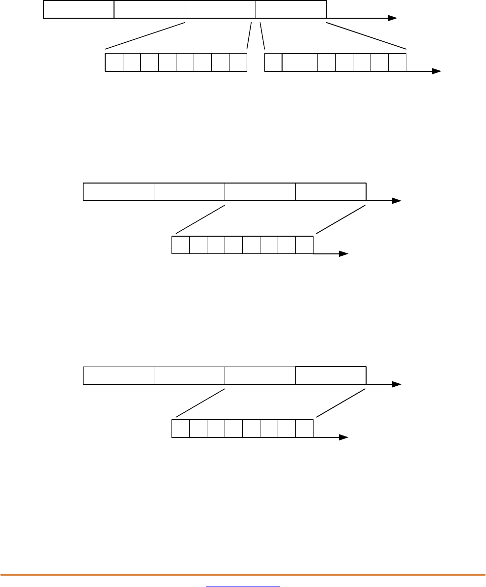
NOIP1SN1300A
www.onsemi.com
47
Data order for P2−SN/SE: CMOS Interface Version
To read out the image data through the parallel CMOS
output, the pixel array is divided in kernels. The kernel size
is eight pixels in x−direction by one pixel in y−direction.
Figure 35 on page 40 indicates how the kernels are
organized.
The data order of this image data on the data output
channels depends on the subsampling mode.
• P2−SN/SE: No Subsampling
The image data is read out in kernels of eight pixels in
x−direction by one pixel in y−direction.
Figure 47 shows the pixel sequence of a kernel which is
read out over the single CMOS output channel. The pixel
order is different for even and odd kernel positions.
Figure 47. P2−SN/SE: Data Output Order without Subsampling
kernel 12 kernel 15kernel 14kernel 13
0 1642 3 75
pixel # (even kernel)
7 6135 4 02
pixel # (odd kernel)
time
time
• P2−SN: Subsampling On Monochrome Sensor
To read out the image data with subsampling enabled on
a monochrome sensor, two neighboring kernels are
combined to a single kernel of 16 pixels in the x−direction
and one pixel in the y−direction. Only the pixels at the even
pixel positions inside that kernel are read out. Figure 48
shows the data order
Note that there is no difference in data order for even/odd
kernel numbers, as opposed to the ‘no−subsampling’
readout.
Figure 48. P2−SN: Data Output Order with Subsampling on a Monochrome Sensor
kernel 12 kernel 15kernel 14kernel 13
0 14642 12 810
pixel #
time
time
• P2−SE: Subsampling On Color Sensor
To read out the image data with subsampling enabled on
a color sensor, two neighboring kernels are combined to a
single kernel of 16 pixels in the x−direction and one pixel in
the y−direction. Only the pixels 0, 1, 4, 5, 8, 9, 12, and 13 are
read out. Figure 49 shows the data order.
Note that there is no difference in data order for even/odd
kernel numbers, as opposed to the ‘no−subsampling’
readout.
Figure 49. P2−SE: Data Output Order with Subsampling on a Color Sensor
kernel 12 kernel 15kernel 14kernel 13
0 19413 12 85
pixel #
time
time

NOIP1SN1300A
www.onsemi.com
48
REGISTER MAP
The table below represents the register map for the
NOIP1xx1300A part. Deviating default values for the
NOIP1xx0500A and NOIP1xx0300A are mentioned
between brackets (“[ ]”).
Table 28. REGISTER MAP
Address
Offset
Address Bit Field Register Name
Default
(Hex)
Default Description Type
Chip ID [Block Offset: 0]
0 0 chip_id 0x50D0 20688 Chip ID Status
[15:0] id 0x50D0 20688 Chip ID
1 1 reserved 0x0001
0x0201
0x0101
1
[513,
257]
Reserved Status
[3:0] reserved 0x1 1 Reserved
[9:8] resolution 0x0
[0x2,
0x1]
0 [2, 1] Sensor Resolution
0x0: PYTHON1300,
0x1: PYTHON300
0x2: PYTHON500
[11:10] reserved 0x0 0 Reserved
2 2 chip_configuration 0x0000 0 Chip General Configuration RW
[0] color 0x0 0 Color/Monochrome Configuration
‘0’: Monochrome
‘1’: Color
[1] parallel 0x0 0 LVDS/Parallel Mode Selector
‘0’: LVDS
‘1’: Parallel
Reset Generator [Block Offset: 8]
0 8 soft_reset_pll 0x0099 153 PLL Soft Reset Configuration RW
[3:0] pll_soft_reset 0x9 9 PLL Reset
0x9: Soft Reset State
others: Operational
[7:4] pll_lock_soft_reset 0x9 9 PLL Lock Detect Reset
0x9: Soft Reset State
others: Operational
1 9 soft_reset_cgen 0x0009 9 Clock Generator Soft Reset RW
[3:0] cgen_soft_reset 0x9 9 Clock Generator Reset
0x9: Soft Reset State
others: Operational
2 10 soft_reset_analog 0x0999 2457 Analog Block Soft Reset RW
[3:0] mux_soft_reset 0x9 9 Column MUX Reset
0x9: Soft Reset State
others: Operational
[7:4] afe_soft_reset 0x9 9 AFE Reset
0x9: Soft Reset State
others: Operational
[11:8] ser_soft_reset 0x9 9 Serializer Reset
0x9: Soft Reset State
others: Operational
PLL [Block Offset: 16]
0 16 power_down 0x0004 4 PLL Configuration RW
[0] pwd_n 0x0 0 PLL Power Down
‘0’: Power Down,
‘1’: Operational
[1] enable 0x0 0 PLL Enable
‘0’: disabled,
‘1’: enabled
[2] bypass 0x1 1 PLL Bypass
‘0’: PLL Active,
‘1’: PLL Bypassed

NOIP1SN1300A
www.onsemi.com
49
Table 28. REGISTER MAP
Address
Offset
TypeDescriptionDefault
Default
(Hex)
Register NameBit Field
Address
1 17 reserved 0x2113 8467 Reserved RW
[7:0] reserved 0x13 19 Reserved
[12:8] reserved 0x1 1 Reserved
[14:13] reserved 0x1 1 Reserved
I/O [Block Offset: 20]
0 20 config1 0x0000 0 IO Configuration RW
[0] clock_in_pwd_n 0x0 0 Power down Clock Input
[9:8] reserved 0x0 0 Reserved
[10] reserved 0x0 0 Reserved
PLL Lock Detector [Block Offset: 24]
0 24 pll_lock 0x0000 0 PLL Lock Indication Status
[0] lock 0x0 0 PLL Lock Indication
2 26 reserved 0x2280 8832 Reserved RW
[7:0] reserved 0x80 128 Reserved
[10:8] reserved 0x2 2 Reserved
[14:12] reserved 0x2 2 Reserved
3 27 reserved 0x3D2D 15661 Reserved RW
[7:0] reserved 0x2D 45 Reserved
[15:8] reserved 0x3D 61 Reserved
Clock Generator [Block Offset: 32]
0 32 config0 0x0004 4 Clock Generator Configuration RW
[0] enable_analog 0x0 0 Enable analogue clocks
‘0’: disabled,
‘1’: enabled
[1] enable_log 0x0 0 Enable logic clock
‘0’: disabled,
‘1’: enabled
[2] select_pll 0x1 1 Input Clock Selection
‘0’: Select LVDS clock input,
‘1’: Select PLL clock input
[3] adc_mode 0x0 0 Set operation mode of CGEN block
‘0’: divide by 5 mode (10-bit mode),
‘1’: divide by 4 mode (8-bit mode)
[5:4] mux 0x0 0 Multiplex Mode
[11:8] reserved 0x0 0 Reserved
[14:12] reserved 0x0 0 Reserved
General Logic [Block Offset: 34]
0 34 config0 0x0000 0 Clock Generator Configuration RW
[0] enable 0x0 0 Logic General Enable Configuration
‘0’: Disable
‘1’: Enable
Image Core [Block Offset: 40]
0 40 image_core_config0 0x0000 0 Image Core Configuration RW
[0] imc_pwd_n 0x0 0 Image Core Power Down
‘0’: powered down,
‘1’: powered up
[1] mux_pwd_n 0x0 0 Column Multiplexer Power Down
‘0’: powered down,
‘1’: powered up

NOIP1SN1300A
www.onsemi.com
50
Table 28. REGISTER MAP
Address
Offset
TypeDescriptionDefault
Default
(Hex)
Register NameBit Field
Address
[2] colbias_enable 0x0 0 Bias Enable
‘0’: disabled
‘1’: enabled
1 41 image_core_config1 0x0B5A 2906 Image Core Configuration RW
[3:0] dac_ds 0xA 10 Double Slope Reset Level
[7:4] dac_ts 0x5 5 Triple Slope Reset Level
[10:8] reserved 0x3 3 Reserved
[12:11] reserved 0x1 1 Reserved
[13] reserved 0x0 0 Reserved
[14] reserved 0x0 0 Reserved
[15] reserved 0x0 0 Reserved
2 42 reserved 0x0001 1 Reserved RW
[0] reserved 0x1 1 Reserved
[1] reserved 0x0 0 Reserved
[6:4] reserved 0x0 0 Reserved
[10:8] reserved 0x0 0 Reserved
[15:12] reserved 0x0 0 Reserved
3 43 reserved 0x0000 0 Reserved RW
[0] reserved 0x0 0 Reserved
[1] reserved 0x0 0 Reserved
[2] reserved 0x0 0 Reserved
[3] reserved 0x0 0 Reserved
[6:4] reserved 0x0 0 Reserved
[15:7] reserved 0x0 0 Reserved
AFE [Block Offset: 48]
0 48 power_down 0x0000 0 AFE Configuration RW
[0] pwd_n 0x0 0 Power down for AFE’s
‘0’: powered down,
‘1’: powered up
Bias [Block Offset: 64]
0 64 power_down 0x0000 0 Bias Power Down Configuration RW
[0] pwd_n 0x0 0 Power down bandgap
‘0’: powered down,
‘1’: powered up
1 65 configuration 0x888B 34955 Bias Configuration RW
[0] extres 0x1 1 External Resistor Selection
‘0’: internal resistor,
‘1’: external resistor
[3:1] reserved 0x5 5 Reserved
[7:4] imc_colpc_ibias 0x8 8 Column Precharge ibias Configuration
[11:8] imc_colbias_ibias 0x8 8 Column Bias ibias Configuration
[15:12] cp_ibias 0x8 8 Charge Pump Bias
2 66 afe_bias 0x53C8 21448 AFE Bias Configuration RW
[3:0] afe_ibias 0x8 8 AFE ibias Configuration
[7:4] afe_adc_iref 0xC 12 ADC iref Configuration
[14:8] afe_pga_iref 0x53 83 PGA iref Configuration
3 67 mux_bias 0x8888 34952 Column Multiplexer Bias Configuration RW
[3:0] mux_25u_stage1 0x8 8 Column Multiplexer Stage 1 Bias Configuration

NOIP1SN1300A
www.onsemi.com
51
Table 28. REGISTER MAP
Address
Offset
TypeDescriptionDefault
Default
(Hex)
Register NameBit Field
Address
[7:4] mux_25u_stage2 0x8 8 Column Multiplexer Stage 2 Bias Configuration
[11:8] mux_25u_delay 0x8 8 Column Multiplexer Delay Bias Configuration
[15:12] reserved 0x8 8 Reserved
4 68 lvds_bias 0x0088 136 LVDS Bias Configuration RW
[3:0] lvds_ibias 0x8 8 LVDS Ibias
[7:4] lvds_iref 0x8 8 LVDS Iref
5 69 adc_bias 0x0088 136 LVDS Bias Configuration RW
[3:0] imc_vsfdmed_ibias 0x8 8 VSFD Medium Bias
[7:4] adcref_ibias 0x8 8 ADC Reference Bias
6 70 reserved 0x8888 34952 Reserved RW
[3:0] reserved 0x8 8 Reserved
[7:4] reserved 0x8 8 Reserved
[11:8] reserved 0x8 8 Reserved
[15:12] reserved 0x8 8 Reserved
7 71 reserved 0x8888 34952 Reserved RW
[15:0] reserved 0x8888 34952 Reserved
Charge Pump [Block Offset: 72]
0 72 configuration 0x2220 8736 Charge Pump Configuration RW
[0] trans_pwd_n 0x0 0 PD Trans Charge Pump Enable
‘0’: disabled,
‘1’: enabled
[1] resfd_calib_pwd_n 0x0 0 FD Charge Pump Enable
‘0’: disabled,
‘1’: enabled
[2] sel_sample_pwd_n 0x0 0 Select/Sample Charge Pump Enable
‘0’: disabled
‘1’: enabled
[6:4] trans_trim 0x2 2 PD Trans Charge Pump Trim
[10:8] resfd_calib_trim 0x2 2 FD Charge Pump Trim
[14:12] sel_sample_trim 0x2 2 Select/Sample Charge Pump Trim
Charge Pump [Block Offset: 80]
reserved Reserved
0 80 reserved 0x0000 0 Reserved RW
[1:0] reserved 0x0 0 Reserved
[3:2] reserved 0x0 0 Reserved
[5:4] reserved 0x0 0 Reserved
[7:6] reserved 0x0 0 Reserved
[9:8] reserved 0x0 0 Reserved
1 81 reserved 0x8881 34945 Reserved RW
[15:0] reserved 0x8881 34945 Reserved
Temperature Sensor [Block Offset: 96]
0 96 enable 0x0000 0 Temperature Sensor Configuration RW
[0] enable 0x0 0 Temperature Diode Enable
‘0’: disabled,
‘1’: enabled
[1] reserved 0x0 0 Reserved
[2] reserved 0x0 0 Reserved

NOIP1SN1300A
www.onsemi.com
52
Table 28. REGISTER MAP
Address
Offset
TypeDescriptionDefault
Default
(Hex)
Register NameBit Field
Address
[3] reserved 0x0 0 Reserved
[4] reserved 0x0 0 Reserved
[5] reserved 0x0 0 Reserved
[13:8] offset 0x0 0 Temperature Offset (signed)
1 97 temp 0x0000 0 Temperature Sensor Status Status
[7:0] temp 0x00 0 Temperature Readout
Reserved [Block Offset: 104]
reserved Reserved
0 104 reserved 0x0000 0 Reserved RW
[15:0] reserved 0x0 0 Reserved
1 105 reserved 0x0000 0 Reserved RW
[1:0] reserved 0x0 0 Reserved
[6:2] reserved 0x0 0 Reserved
[7] reserved 0x0 0 Reserved
[9:8] reserved 0x0 0 Reserved
[14:10] reserved 0x0 0 Reserved
[15] reserved 0x0 0 Reserved
2 106 reserved 0x0000 0 Reserved Status
[15:0] reserved 0x0000 0 Reserved
3 107 reserved 0x0000 0 Reserved Status
[15:0] reserved 0x0000 0 Reserved
4 108 reserved 0x0000 0 Reserved Status
[15:0] reserved 0x0000 0 Reserved
5 109 reserved 0x0000 0 Reserved Status
[15:0] reserved 0x0000 0 Reserved
6 110 reserved 0x0000 0 Reserved Status
[15:0] reserved 0x0000 0 Reserved
7 111 reserved 0x0000 0 Reserved Status
[15:0] reserved 0x0000 0 Reserved
Serializers/LVDS/IO [Block Offset: 112]
0 112 power_down 0x0000 0 LVDS Power Down Configuration RW
[0] clock_out_pwd_n 0x0 0 Power down for Clock Output.
‘0 ’: powered down,
‘1’: powered up
[1] sync_pwd_n 0x0 0 Power down for Sync channel
‘0’: powered down,
‘1’: powered up
[2] data_pwd_n 0x0 0 Power down for data channels (4 channels)
‘0’: powered down,
‘1’: powered up
Sync Words [Block Offset: 116]
4 116 trainingpattern 0x03A6 934 Data Formating - Training Pattern RW
[9:0] trainingpattern 0x3A6 934 Training pattern sent on Data channels during
idle mode. This data is used to perform word
alignment on the LVDS data channels.
5 117 sync_code0 0x002A 42 LVDS Power Down Configuration RW
[6:0] frame_sync_0 0x02A 42 Frame Sync Code LSBs - Even kernels

NOIP1SN1300A
www.onsemi.com
53
Table 28. REGISTER MAP
Address
Offset
TypeDescriptionDefault
Default
(Hex)
Register NameBit Field
Address
6 118 sync_code1 0x0015 21 Data Formating - BL Indication RW
[9:0] bl_0 0x015 21 Black Pixel Identification Sync Code - Even
kernels
7 119 sync_code2 0x0035 53 Data Formating - IMG Indication RW
[9:0] img_0 0x035 53 Valid Pixel Identification Sync Code - Even
kernels
8 120 sync_code3 0x0025 37 Data Formating - IMG Indication RW
[9:0] ref_0 0x025 37 Reference Pixel Identification Sync Code -
Even kernels
9 121 sync_code4 0x002A 42 LVDS Power Down Configuration RW
[6:0] frame_sync_1 0x02A 42 Frame Sync Code LSBs - Odd kernels
10 122 sync_code5 0x0015 21 Data Formating - BL Indication RW
[9:0] bl_1 0x015 21 Black Pixel Identification Sync Code -
Odd kernels
11 123 sync_code6 0x0035 53 Data Formating - IMG Indication RW
[9:0] img_1 0x035 53 Valid Pixel Identification Sync Code -
Odd kernels
12 124 sync_code7 0x0025 37 Data Formating - IMG Indication RW
[9:0] ref_1 0x025 37 Reference Pixel Identification Sync Code -
Odd kernels
13 125 sync_code8 0x0059 89 Data Formating - CRC Indication RW
[9:0] crc 0x059 89 CRC Value Identification Sync Code
14 126 sync_code9 0x03A6 934 Data Formating - TR Indication RW
[9:0] tr 0x3A6 934 Training Value Identification Sync Code
Data Block [Block Offset: 128]
0 128 blackcal 0x4008 16392 Black Calibration Configuration RW
[7:0] black_offset 0x08 8 Desired black level at output
[10:8] black_samples 0x0 0 Black pixels taken into account for black
calibration.
Total samples = 2**black_samples
[14:11] reserved 0x8 8 Reserved
[15] crc_seed 0x0 0 CRC Seed
‘0’: All-0
‘1’: All-1
1 129 general_configuration 0x0001 1 Black Calibration and Data Formating
Configuration
RW
[0] auto_blackcal_enable 0x1 1 Automatic blackcalibration is enabled when 1,
bypassed when 0
[9:1] blackcal_offset 0x00 0 Black Calibration offset used when au-
to_black_cal_en = ‘0’.
[10] blackcal_offset_dec 0x0 0 blackcal_offset is added when 0, subtracted
when 1
[11] reserved 0x0 0 Reserved
[12] reserved 0x0 0 Reserved
[13] 8bit_mode 0x0 0 Shifts window ID indications by 4 cycles.
‘0’: 10 bit mode,
‘1’: 8 bit mode
[14] ref_mode 0x0 0 Data contained on reference lines:
‘0’: reference pixels
‘1’: black average for the corresponding data
channel
[15] ref_bcal_enable 0x0 0 Enable black calibration on reference lines
‘0’: Disabled
‘1’: Enabled

NOIP1SN1300A
www.onsemi.com
54
Table 28. REGISTER MAP
Address
Offset
TypeDescriptionDefault
Default
(Hex)
Register NameBit Field
Address
2 130 trainingpattern 0x000F 15 Data Formating - Training Pattern RW
[0]
bl_frame_valid_en-
able
0x1 1 Assert frame_valid for black lines when ‘1’,
gate frame_valid for black lines when ‘0’.
Parallel output mode only.
[1]
bl_line_valid_enable 0x1 1 Assert line_valid for black lines when ‘1’, gate
line_valid for black lines when ‘0’.
Parallel output mode only.
[2]
ref_frame_valid_en-
able
0x1 1 Assert frame_valid for ref lines when ‘1’, gate
frame_valid for black lines when ‘0’.
Parallel output mode only.
[3] ref_line_valid_enable 0x1 1 Assert line_valid for ref lines when ‘1’, gate
line_valid for black lines when ‘0’.
Parallel output mode only.
[4] frame_valid_mode 0x0 0 Behaviour of frame_valid strobe between
overhead lines when [0] and/or [1] is
deasserted:
‘0’: retain frame_valid deasserted between
lines
‘1’: assert frame_valid between lines
[8] reserved 0x0 0 Reserved
8 136 blackcal_error0 0x0000 0 Black Calibration Status Status
[15:0] blackcal_error[15:0] 0x0000 0 Black Calibration Error. This flag is set when
not enough black samples are availlable.
Black Calibration shall not be valid.
Channels 0-16
(channels 0-7 for PYTHON1300)
9 137 reserved 0x0000 0 Reserved Status
[15:0] reserved 0x0000 0 Reserved
10 138 reserved 0x0000 0 Reserved Status
[15:0] reserved 0x0000 0 Reserved
11 139 reserved 0x0000 0 Reserved Status
[15:0] reserved 0x0000 0 Reserved
12 140 reserved 0x0000 0 Reserved RW
[15:0] reserved 0x0000 0 Reserved
13 141 reserved 0xFFFF 65535 Reserved RW
[15:0] reserved 0xFFFF 65535 Reserved
16 144 test_configuration 0x0000 0 Data Formating Test Configuration RW
[0] testpattern_en 0x0 0 Insert synthesized testpattern when ‘1’
[1] inc_testpattern 0x0 0 Incrementing testpattern when ‘1’, constant
testpattern when ’0’
[2] prbs_en 0x0 0 Insert PRBS when ‘1’
[3] frame_testpattern 0x0 0 Frame test patterns when ‘1’, unframed test-
patterns when ‘0’
[4] reserved 0x0 0 Reserved
17 145 reserved 0x0000 0 Reserved RW
[15:0] reserved Reserved
18 146 test_configuration0 0x0100 256 Data Formating Test Configuration RW
[7:0] testpattern0_lsb 0x00 0 Testpattern used on datapath #0 when
testpattern_en = ‘1’.
Note: Most significant bits are configured in
register 150.
[15:8] testpattern1_lsb 0x01 1 Testpattern used on datapath #1 when
testpattern_en = ‘1’.
Note: Most significant bits are configured in
register 150.

NOIP1SN1300A
www.onsemi.com
55
Table 28. REGISTER MAP
Address
Offset
TypeDescriptionDefault
Default
(Hex)
Register NameBit Field
Address
19 147 test_configuration1 0x0302 770 Data Formating Test Configuration RW
[7:0] testpattern2_lsb 0x02 2 Testpattern used on datapath #2 when
testpattern_en = ‘1’.
Note: Most significant bits are configured in
register 150.
[15:8] testpattern3_lsb 0x03 3 Testpattern used on datapath #3 when
testpattern_en = ‘1’.
Note: Most significant bits are configured in
register 150.
20 148 reserved 0x0504 1284 Reserved RW
[7:0] reserved 0x04 4 Reserved
[15:8] reserved 0x05 5 Reserved
21 149 reserved 0x0706 1798 Reserved RW
[7:0] reserved 0x06 6 Reserved
[15:8] reserved 0x07 7 Reserved
22 150 test_configuration16 0x0000 0 Data Formating Test Configuration RW
[1:0] testpattern0_msb 0x0 0 Testpattern used when testpattern_en = ‘1’
[3:2] testpattern1_msb 0x0 0 Testpattern used when testpattern_en = ‘1’
[5:4] testpattern2_msb 0x0 0 Testpattern used when testpattern_en = ‘1’
[7:6] testpattern3_msb 0x0 0 Testpattern used when testpattern_en = ‘1’
[9:8] reserved 0x0 0 Reserved
[11:10] reserved 0x0 0 Reserved
[13:12] reserved 0x0 0 Reserved
[15:14] reserved 0x0 0 Reserved
26 154 reserved 0x0000 0 Reserved RW
[15:0] reserved 0x0000 0 Reserved
27 155 reserved 0x0000 0 Reserved RW
[15:0] reserved 0x0000 0 Reserved
AEC [Block Offset: 160]
0 160 configuration 0x0010 16 AEC Configuration RW
[0] enable 0x0 0 AEC Enable
[1] restart_filter 0x0 0 Restart AEC filter
[2] freeze 0x0 0 Freeze AEC filter and enforcer gains
[3] pixel_valid 0x0 0 Use every pixel from channel when 0, every
4th pixel when 1
[4] amp_pri 0x1 1 Column amplifier gets higher priority than AFE
PGA in gain distribution if 1. Vice versa if 0
1 161 intensity 0x60B8 24760 AEC Configuration RW
[9:0] desired_intensity 0xB8 184 Target average intensity
[15:10] reserved 0x018 24 Reserved
2 162 red_scale_factor 0x0080 128 Red Scale Factor RW
[9:0] red_scale_factor 0x80 128 Red Scale Factor
3.7 unsigned
3 163 green1_scale_factor 0x0080 128 Green1 Scale Factor RW
[9:0] green1_scale_factor 0x80 128 Green1 Scale Factor
3.7 unsigned
4 164 green2_scale_factor 0x0080 128 Green2 Scale Factor RW
[9:0] green2_scale_factor 0x80 128 Green2 Scale Factor
3.7 unsigned

NOIP1SN1300A
www.onsemi.com
56
Table 28. REGISTER MAP
Address
Offset
TypeDescriptionDefault
Default
(Hex)
Register NameBit Field
Address
5 165 blue_scale_factor 0x0080 128 Blue Scale Factor RW
[9:0] blue_scale_factor 0x80 128 Blue Scale Factor
3.7 unsigned
6 166 reserved 0x03FF 1023 Reserved RW
[15:0] reserved 0x03FF 1023 Reserved
7 167 reserved 0x0080 2048 Reserved RW
[1:0] reserved 0x0 0 Reserved
[3:2] reserved 0x0 0 Reserved
[15:4] reserved 0x080 128 Reserved
8 168 min_exposure 0x0001 1 Minimum Exposure Time RW
[15:0] min_exposure 0x0001 1 Minimum Exposure Time
9 169 min_gain 0x0800 2048 Minimum Gain RW
[1:0] min_mux_gain 0x0 0 Minimum Column Amplifier Gain
[3:2] min_afe_gain 0x0 0 Minimum AFE PGA Gain
[15:4] min_digital_gain 0x080 128 Minimum Digital Gain
5.7 unsigned
10 170 max_exposure 0x03FF 1023 Maximum Exposure Time RW
[15:0] max_exposure 0x03FF 1023 Maximum Exposure Time
11 171 max_gain 0x100D 4109 Maximum Gain RW
[1:0] max_mux_gain 0x1 1 Maximum Column Amplifier Gain
[3:2] max_afe_gain 0x3 3 Maximum AFE PGA Gain
[15:4] max_digital_gain 0x100 256 Maximum Digital Gain
5.7 unsigned
12 172 reserved 0x0083 131 Reserved RW
[7:0] reserved 0x083 131 Reserved
[13:8] reserved 0x00 0 Reserved
[15:14] reserved 0x0 0 Reserved
13 173 reserved 0x2824 10276 Reserved RW
[7:0] reserved 0x024 36 Reserved
[15:8] reserved 0x028 40 Reserved
14 174 reserved 0x2A96 10902 Reserved RW
[3:0] reserved 0x6 6 Reserved
[7:4] reserved 0x9 9 Reserved
[11:8] reserved 0xA 10 Reserved
[15:12] reserved 0x2 2 Reserved
15 175 reserved 0x0080 128 Reserved RW
[9:0] reserved 0x080 128 Reserved
16 176 reserved 0x0100 256 Reserved RW
[9:0] reserved 0x100 256 Reserved
17 177 reserved 0x0100 256 Reserved RW
[9:0] reserved 0x100 256 Reserved
18 178 reserved 0x0080 128 Reserved RW
[9:0] reserved 0x080 128 Reserved
19 179 reserved 0x00AA 170 Reserved RW
[9:0] reserved 0x0AA 170 Reserved

NOIP1SN1300A
www.onsemi.com
57
Table 28. REGISTER MAP
Address
Offset
TypeDescriptionDefault
Default
(Hex)
Register NameBit Field
Address
20 180 reserved 0x0100 256 Reserved RW
[9:0] reserved 0x100 256 Reserved
21 181 reserved 0x0155 341 Reserved RW
[9:0] reserved 0x155 341 Reserved
24 184 total_pixels0 0x0000 0 AEC Status Status
[15:0] total_pixels[15:0] 0x0000 0 Total number of pixels sampled for Average,
LSB
25 185 total_pixels1 0x0000 0 AEC Status Status
[7:0] total_pixels[23:16] 0x0 0 Total number of pixels sampled for Average,
MSB
26 186 average_status 0x0000 0 ASE Status Status
[9:0] average 0x000 0 AEC Average Status
[12] avg_locked 0x0 0 AEC Average Lock Status
27 187 exposure_status 0x0000 0 ASE Status Status
[15:0] exposure 0x0000 0 AEC Exposure Status
28 188 gain_status 0x0000 0 ASE Status Status
[1:0] mux_gain 0x0 0 AEC MUX Gain Status
[3:2] afe_gain 0x0 0 AEC AFE Gain Status
[15:4] digital_gain 0x000 0 AEC Digital Gain Status
5.7 unsigned
29 189 reserved 0x0000 0 Reserved Status
[12:0] reserved 0x000 0 Reserved
[13] reserved 0x0 0 Reserved
Sequencer [Block Offset: 192]
0 192 general_configuration 0x0000 0 Sequencer General Configuration RW
[0] enable 0x0 0 Enable sequencer
‘0’: Idle,
‘1’: enabled
[1] operation selection 0x0 0 ‘0’: Global Shutter
[2] zero_rot_enable 0x0 0 Zero ROT mode Selection.
‘0’: Normal ROT,
‘1’: Zero ROT’
[3] reserved 0x0 0 Reserved
[4] triggered_mode 0x0 0 Triggered Mode Selection
‘0’: Normal Mode,
‘1’: Triggered Mode
[5] slave_mode 0x0 0 Master/Slave Selection
‘0’: master,
‘1’: slave
[6] nzrot_xsm_delay_en-
able
0x0 0 Insert delay between end of ROT and start of
readout in normal ROT readout mode if ‘1’.
ROT delay is defined by register xsm_delay
[7] subsampling 0x0 0 Subsampling mode selection
‘0’: no subsampling,
‘1’: subsampling
[8] binning 0x0 0 Binning mode selection
‘0’: no binning,
‘1’: binning
[10] roi_aec_enable 0x0 0 Enable windowing for AEC Statistics.
‘0’: Subsample all windows
‘1’: Subsample configured window
[13:11] monitor_select 0x0 0 Control of the monitor pins
[14] reserved 0x0 0 Reserved

NOIP1SN1300A
www.onsemi.com
58
Table 28. REGISTER MAP
Address
Offset
TypeDescriptionDefault
Default
(Hex)
Register NameBit Field
Address
[15] reserved 0x0 0 Reserved
1 193 delay_configuration 0x0000 0 Sequencer Delay Configuration RW
[7:0] reserved 0x00 0 Reserved
[15:8] xsm_delay 0x00 0 Delay between ROT start and X-readout (Zero
ROT mode)
Delay between ROT end and X-readout
(Normal ROT mode with
nzrot_xsm_delay_enable=‘1’)
2 194 integration_control 0x00E4 228 Integration Control RW
[0] dual_slope_enable 0x0 0 Enable Dual Slope
[1] triple_slope_enable 0x0 0 Enable Triple Slope
[2] fr_mode 0x1 1 Representation of fr_length.
‘0’: reset length
‘1’: frame length
[4] int_priority 0x0 0 Integration Priority
‘0’: Frame readout has priority over integration
‘1’: Integration End has priority over frame
readout
[5] halt_mode 0x1 1 The current frame will be completed when the
sequencer is disabled and halt_mode = ‘1’.
When ‘0’, the sensor stops immediately when
disabled, without finishing the current frame.
[6] fss_enable 0x1 1 Generation of Frame Sequence Start Sync
code (FSS)
‘0’: No generation of FSS
‘1’: Generation of FSS
[7] fse_enable 0x1 1 Generation of Frame Sequence End Sync
code (FSE)
‘0’: No generation of FSE
‘1’: Generation of FSE
[8] reverse_y 0x0 0 Reverse readout
‘0’: bottom to top readout
‘1’: top to bottom readout
[9] reserved 0x0 0 Reserved
[11:10] subsampling_mode 0x0 0 Subsampling mode
“00”: Subsampling in x and y (VITA
compatible)
“01”: Subsampling in x, not y
“10”: Subsampling in y, not x
“11”: Subsampling in x an y
[13:12] binning_mode 0x0 0 Binning mode
“00”: Binning in x and y (VITA compatible)
“01”: Binning in x, not y
“10”: Binning in y, not x
“11”: Binning in x an y
[14] reserved 0x0 0 Reserved
[15] reserved 0x0 0 Reserved
3 195 roi_active0_0 0x0001 1 Active ROI Selection RW
[7:0] roi_active0[7:0] 0x01 1 Active ROI Selection
[0] Roi0 Active
[1] Roi1 Active
...
[7] Roi7 Active
4 196 reserved 0x0000 0 Reserved RW
[15:0] reserved 0x0000 0 Reserved
5 197 black_lines 0x0102 258 Black Line Configuration RW
[7:0] black_lines 0x02 2 Number of black lines. Minimum is 1.
Range 1-255

NOIP1SN1300A
www.onsemi.com
59
Table 28. REGISTER MAP
Address
Offset
TypeDescriptionDefault
Default
(Hex)
Register NameBit Field
Address
[12:8] gate_first_line 0x1 1 Blank out first lines
0: no blank
1-31: blank 1-31 lines
6 198 reserved 0x0000 0 Reserved RW
[11:0] reserved 0x000 0 Reserved
7 199 mult_timer0 0x0001 1 Exposure/Frame Rate Configuration RW
[15:0] mult_timer0 0x0001 1 Mult Timer
Defines granularity (unit = 1/PLL clock) of
exposure and reset_length
8 200 fr_length0 0x0000 0 Exposure/Frame Rate Configuration RW
[15:0] fr_length0 0x0000 0 Frame/Reset length
Reset length when fr_mode = ‘0’, Frame
Length when fr_mode = ‘1’
Granularity defined by mult_timer
9 201 exposure0 0x0000 0 Exposure/Frame Rate Configuration RW
[15:0] exposure0 0x0000 0 Exposure Time
Granularity defined by mult_timer
10 202 exposure_ds0 0x0000 0 Exposure/Frame Rate Configuration RW
[15:0] exposure_ds0 0x0000 0 Exposure Time (Dual Slope)
Granularity defined by mult_timer
11 203 exposure_ts0 0x0000 0 Exposure/Frame Rate Configuration RW
[15:0] exposure_ts0 0x0000 0 Exposure Time (Triple Slope)
Granularity defined by mult_timer
12 204 gain_configuration0 0x01E3 483 Gain Configuration RW
[4:0] mux_gainsw0 0x03 3 Column Gain Setting
[12:5] afe_gain0 0xF 15 AFE Programmable Gain Setting
[13] gain_lat_comp 0x0 0 Postpone gain update by 1 frame when ‘1’ to
compensate for exposure time updates laten-
cy.
Gain is applied at start of next frame if ‘0’
13 205 digital_gain
_configuration0
0x0080 128 Gain Configuration RW
[11:0] db_gain0 0x080 128 Digital Gain
14 206 sync_configuration 0x037F 895 Synchronization Configuration RW
[0] sync_rs_x_length 0x1 1 Update of rs_x_length will not be sync’ed at
start of frame when ‘0’
[1] sync_black_lines 0x1 1 Update of black_lines will not be sync’ed at start
of frame when ‘0’
[2] sync_dummy_lines 0x1 1 Update of dummy_lines will not be sync’ed at
start of frame when ‘0’
[3] sync_exposure 0x1 1 Update of exposure will not be sync’ed at start of
frame when ‘0’
[4] sync_gain 0x1 1 Update of gain settings (gain_sw, afe_gain) will
not be sync’ed at start of frame when ‘0’
[5] sync_roi 0x1 1 Update of roi updates (active_roi) will not be
sync’ed at start of frame when ‘0’
[6] sync_ref_lines 0x1 1 Update of ref_lines will not be sync’ed at start of
frame when ‘0’
[8] blank_roi_switch 0x1 1 Blank first frame after ROI switching
[9] blank
_subsampling_ss
0x1 1 Blank first frame after subsampling/binning
mode.

NOIP1SN1300A
www.onsemi.com
60
Table 28. REGISTER MAP
Address
Offset
TypeDescriptionDefault
Default
(Hex)
Register NameBit Field
Address
[10] expos-
ure_sync_mode
0x0 0 When ‘0’, exposure configurations are sync’ed
at the start of FOT. When ‘1’, exposure
configurations sync is disabled (continuously
syncing). This mode is only relevant for Trig-
gered snapshot - master mode, where the ex-
posure configurations are sync’ed at the start
of exposure rather than the start of FOT. For
all other modes it should be set to ‘0’.
Note: Sync is still postponed if
sync_exposure=‘0’.
15 207 ref_lines 0x0000 0 Reference Line Configuration RW
[7:0] ref_lines 0x00 0 Number of Reference Lines
0-255
16 208 reserved 0x9F00 40704 Reserved RW
[7:0] reserved 0x00 0 Reserved
[15:8] reserved 0x9F 159 Reserved
19 211 reserved 0x0E5B 3675 Reserved RW
[0] reserved 0x1 1 Reserved
[1] reserved 0x1 1 Reserved
[2] reserved 0x0 0 Reserved
[3] reserved 0x1 1 Reserved
[6:4] reserved 0x5 5 Reserved
[15:8] reserved 0xE 14 Reserved
20 212 reserved 0x0000 0 Reserved RW
[12:0] reserved 0x0000 0 Reserved
[15] reserved 0x0 0 Reserved
21 213 reserved 0x03FF 1023 Reserved RW
[12:0] reserved 0x03FF 1023 Reserved
22 214 reserved 0x0000 0 Reserved RW
[7:0] reserved 0x00 0 Reserved
[15:8] reserved 0x0 0 Reserved
23 215 reserved 0x0103 259 Reserved RW
[0] reserved 0x1 1 Reserved
[1] reserved 0x1 1 Reserved
[2] reserved 0x0 0 Reserved
[3] reserved 0x0 0 Reserved
[4] reserved 0x0 0 Reserved
[5] reserved 0x0 0 Reserved
[6] reserved 0x0 0 Reserved
[7] reserved 0x0 0 Reserved
[8] reserved 0x1 1 Reserved
[9] reserved 0x0 0 Reserved
[10] reserved 0x0 0 Reserved
[11] reserved 0x0 0 Reserved
[12] reserved 0x0 0 Reserved
[13] reserved 0x0 0 Reserved
[14] reserved 0x0 0 Reserved
24 216 reserved 0x7F08 32520 Reserved RW
[6:0] reserved 0x08 8 Reserved

NOIP1SN1300A
www.onsemi.com
61
Table 28. REGISTER MAP
Address
Offset
TypeDescriptionDefault
Default
(Hex)
Register NameBit Field
Address
[14:8] reserved 0x7F 127 Reserved
25 217 reserved 0x4444 17476 Reserved RW
[6:0] reserved 0x44 68 Reserved
[14:8] reserved 0x44 68 Reserved
26 218 reserved 0x4444 17476 Reserved RW
[6:0] reserved 0x44 68 Reserved
[14:8] reserved 0x44 68 Reserved
27 219 reserved 0x0016 22 Reserved RW
[6:0] reserved 0x016 22 Reserved
[14:8] reserved 0x00 0 Reserved
28 220 lsm_prog_base_ss 0x301F 12319 Sequencer Program Configuration RW
[6:0] lsm_prog_base_ss 0x1F 31 LSM Program start for non−black lines in
Snapshot shutter mode
[14:8] lsm_black_prog_base
_ss
0x30 48 LSM Program start for black lines in Snapshot
shutter mode
29 221 reserved 0x6245 25157 Reserved RW
[6:0] reserved 0x45 69 Reserved
[14:8] reserved 0x62 98 Reserved
30 222 reserved 0x6230 25136 Reserved RW
[6:0] reserved 0x30 48 Reserved
[14:8] reserved 0x62 98 Reserved
31 223 reserved 0x001A 26 Reserved RW
[6:0] reserved 0x1A 26 Reserved
32 224 reserved 0x3E01 15873 Reserved RW
[3:0] reserved 0x1 1 Reserved
[7:4] reserved 0x00 0 Reserved
[8] reserved 0x0 0 Reserved
[9] reserved 0x1 1 Reserved
[10] reserved 0x1 1 Reserved
[11] reserved 0x1 1 Reserved
[12] reserved 0x1 1 Reserved
[13] reserved 0x1 1 Reserved
33 225 reserved 0x5EF1 24305 Reserved RW
[4:0] reserved 0x11 17 Reserved
[9:5] reserved 0x17 23 Reserved
[14:10] reserved 0x17 23 Reserved
[15] reserved 0x0 0 Reserved
34 226 reserved 0x6000 24576 Reserved RW
[4:0] reserved 0x00 0 Reserved
[9:5] reserved 0x00 0 Reserved
[14:10] reserved 0x18 24 Reserved
[15] reserved 0x0 0 Reserved
35 227 reserved 0x0000 0 Reserved RW
[0] reserved 0x0 0 Reserved
[1] reserved 0x0 0 Reserved

NOIP1SN1300A
www.onsemi.com
62
Table 28. REGISTER MAP
Address
Offset
TypeDescriptionDefault
Default
(Hex)
Register NameBit Field
Address
[2] reserved 0x0 0 Reserved
[3] reserved 0x0 0 Reserved
[4] reserved 0x0 0 Reserved
36 228 roi_active0_1 0x0001 1 Active ROI Selection RW
[7:0] roi_active1[7:0] 0x01 1 ROI Configuration
37 229 reserved 0x0000 0 Reserved RW
reserved Reserved
38 230 reserved 0x0001 1 Reserved RW
[15:0] reserved 0x0001 1 Reserved
39 231 reserved 0x0000 0 Reserved RW
[15:0] reserved 0x0000 0 Reserved
40 232 reserved 0x0000 0 Reserved RW
[15:0] reserved 0x0000 0 Reserved
41 233 reserved 0x0000 0 Reserved RW
[15:0] reserved 0x0000 0 Reserved
42 234 reserved 0x0000 0 Reserved RW
[15:0] reserved 0x0000 0 Reserved
43 235 reserved 0x01E3 483 Reserved RW
[4:0] reserved 0x03 3 Reserved
[12:5] reserved 0xF 15 Reserved
44 236 reserved 0x0080 128 Reserved RW
[11:0] reserved 0x080 128 Reserved
45 237 reserved 0x0000 0 Reserved RW
[15:0] reserved 0x0000 0 Reserved
46 238 reserved 0xFFFF 65535 Reserved RW
[15:0] reserved 0xFFFF 65535 Reserved
47 239 reserved 0x0000 0 Reserved RW
[15:0] reserved 0x0 0 Reserved
48 240 x_resolution 0x00A0
[0x0068,
0x0054]
160
[104, 84]
Sequencer Status Status
[7:0] x_resolution 0x00A0
[0x0068,
0x0054]
160
[104, 84]
Sensor x resolution
49 241 y_resolution 0x0400
[0x0268,
0x01F0]
1024
[616,
496]
Sequencer Status Status
[12:0] y_resolution 0x0400
[0x0268,
0x01F0]
1024
[616,
496]
Sensor y resolution
50 242 mult_timer_status 0x0000 0 Sequencer Status Status
[15:0] mult_timer 0x0000 0 Mult Timer Status (Master Snapshot Shutter
only)
51 243 reset_length_status 0x0000 0 Sequencer Status Status
[15:0] reset_length 0x0000 0 Current Reset Length (not in Slave mode)
52 244 exposure_status 0x0000 0 Sequencer Status Status
[15:0] exposure 0x0000 0 Current Exposure Time (not in Slave mode)

NOIP1SN1300A
www.onsemi.com
63
Table 28. REGISTER MAP
Address
Offset
TypeDescriptionDefault
Default
(Hex)
Register NameBit Field
Address
53 245 exposure_ds_status 0x0000 0 Sequencer Status Status
[15:0] exposure_ds 0x0000 0 Current Exposure Time (not in Slave mode)
54 246 exposure_ts_status 0x0000 0 Sequencer Status Status
[15:0] exposure_ts 0x0000 0 Current Exposure Time (not in Slave mode)
55 247 gain_status 0x0000 0 Sequencer Status Status
[4:0] mux_gainsw 0x00 0 Current Column Gain Setting
[12:5] afe_gain 0x00 0 Current AFE Programmable Gain
56 248 digital_gain_status 0x0000 0 Sequencer Status Status
[11:0] db_gain 0x000 0 Digital Gain
[12] dual_slope 0x0 0 Dual Slope Enabled
[13] triple_slope 0x0 0 Triple Slope Enabled
58 250 reserved 0x0423 1059 Reserved RW
[4:0] reserved 0x03 3 Reserved
[9:5] reserved 0x01 1 Reserved
[14:10] reserved 0x01 1 Reserved
59 251 reserved 0x030F 783 Reserved RW
[7:0] reserved 0xF 15 Reserved
[15:8] reserved 0x3 3 Reserved
60 252 reserved 0x0601 1537 Reserved RW
[7:0] reserved 0x1 1 Reserved
[15:8] reserved 0x6 6 Reserved
61 253 roi_aec_configura-
tion0
0x0000 0 AEC ROI Configuration RW
[7:0] x_start 0x00 0 AEC ROI X Start Configuration (used for AEC
statistics when roi_aec_enable=‘1’)
[15:8] x_end 0x00 0 AEC ROI X End Configuration (used for AEC
statistics when roi_aec_enable=‘1’)
62 254 roi_aec_configura-
tion1
0x0000 0 AEC ROI Configuration RW
[12:0] y_start 0x0000 0 AEC ROI Y Start Configuration (used for AEC
statistics when roi_aec_enable=‘1’)
63 255 roi_aec_configura-
tion2
0x0000 0 AEC ROI Configuration RW
[12:0] y_end 0x0000 0 AEC ROI Y End Configuration (used for AEC
statistics when roi_aec_enable=‘1’)
Sequencer ROI [Block Offset: 256]
0 256 roi0_configuration0 0x9F00 40704 ROI Configuration RW
[7:0] x_start 0x00 0 X Start Configuration
[15:8] x_end 0x9F 159 X End Configuration
1 257 roi0_configuration1 0x0000 0 ROI Configuration RW
[12:0] y_start 0x0000 0 Y Start Configuration
2 258 roi0_configuration2 0x03FF 1023 ROI Configuration RW
[12:0] y_end 0x3FF 1023 Y End Configuration
3 259 roi1_configuration0 0x9F00 40704 ROI Configuration RW
[7:0] x_start 0x00 0 X Start Configuration
[15:8] x_end 0x9F 159 X End Configuration

NOIP1SN1300A
www.onsemi.com
64
Table 28. REGISTER MAP
Address
Offset
TypeDescriptionDefault
Default
(Hex)
Register NameBit Field
Address
4 260 roi1_configuration1 0x0000 0 ROI Configuration RW
[12:0] y_start 0x0000 0 Y Start Configuration
5 261 roi1_configuration2 0x03FF 1023 ROI Configuration RW
[12:0] y_end 0x3FF 1023 Y End Configuration
6 262 roi2_configuration0 0x9F00 40704 ROI Configuration RW
[7:0] x_start 0x00 0 X Start Configuration
[15:8] x_end 0x9F 159 X End Configuration
7 263 roi2_configuration1 0x0000 0 ROI Configuration RW
[12:0] y_start 0x0000 0 Y Start Configuration
8 264 roi2_configuration2 0x03FF 1023 ROI Configuration RW
[12:0] y_end 0x3FF 1023 Y End Configuration
9 265 roi3_configuration0 0x9F00 40704 ROI Configuration RW
[7:0] x_start 0x00 0 X Start Configuration
[15:8] x_end 0x9F 159 X End Configuration
10 266 roi3_configuration1 0x0000 0 ROI Configuration RW
[12:0] y_start 0x0000 0 Y Start Configuration
11 267 roi3_configuration2 0x03FF 1023 ROI Configuration RW
[12:0] y_end 0x3FF 1023 Y End Configuration
12 268 roi4_configuration0 0x9F00 40704 ROI Configuration RW
[7:0] x_start 0x00 0 X Start Configuration
[15:8] x_end 0x9F 159 X End Configuration
13 269 roi4_configuration1 0x0000 0 ROI Configuration RW
[12:0] y_start 0x0000 0 Y Start Configuration
14 270 roi4_configuration2 0x03FF 1023 ROI Configuration RW
[12:0] y_end 0x3FF 1023 Y End Configuration
15 271 roi5_configuration0 0x9F00 40704 ROI Configuration RW
[7:0] x_start 0x00 0 X Start Configuration
[15:8] x_end 0x9F 159 X End Configuration
16 272 roi5_configuration1 0x0000 0 ROI Configuration RW
[12:0] y_start 0x0000 0 Y Start Configuration
17 273 roi5_configuration2 0x03FF 1023 ROI Configuration RW
[12:0] y_end 0x3FF 1023 Y End Configuration
18 274 roi6_configuration0 0x9F00 40704 ROI Configuration RW
[7:0] x_start 0x00 0 X Start Configuration
[15:8] x_end 0x9F 159 X End Configuration
19 275 roi6_configuration1 0x0000 0 ROI Configuration RW
[12:0] y_start 0x0000 0 Y Start Configuration
20 276 roi6_configuration2 0x03FF 1023 ROI Configuration RW
[12:0] y_end 0x3FF 1023 Y End Configuration
21 277 roi7_configuration0 0x9F00 40704 ROI Configuration RW
[7:0] x_start 0x00 0 X Start Configuration
[15:8] x_end 0x9F 159 X End Configuration
22 278 roi7_configuration1 0x0000 0 ROI Configuration RW
[12:0] y_start 0x0000 0 Y Start Configuration

NOIP1SN1300A
www.onsemi.com
65
Table 28. REGISTER MAP
Address
Offset
TypeDescriptionDefault
Default
(Hex)
Register NameBit Field
Address
23 279 roi7_configuration2 0x03FF 1023 ROI Configuration RW
[12:0] y_end 0x3FF 1023 Y End Configuration
Sequencer ROI [Block Offset: 384]
0 384 reserved Reserved RW
[15:0] reserved Reserved
..
… …
…
… …
127 511 reserved Reserved RW
[15:0] reserved Reserved

NOIP1SN1300A
www.onsemi.com
66
PACKAGE INFORMATION
Pin List
The PYTHON 300, PYTHON 500, and PYTHON 1300 image sensors are available in an LVDS output configuration
(P1−SN/SE/FN, P3−SN/SE/FN), with the PYTHON 1300 also available in a CMOS output configuration (P2−SN/SE). The
LVDS I/Os comply to the TIA/EIA−644−A Standard and the CMOS I/Os have a 3.3 V signal level. Tables 29 and 30 show
the pin list for both versions.
Table 29. PIN LIST FOR P1−SN/SE/FN, P3−SN/SE/FN LVDS INTERFACE
Pack Pin
No.
Pin Name I/O Type Direction Description
1 vdd_33 Supply 3.3 V Supply
2 mosi CMOS Input SPI Master Out − Slave In
3 miso CMOS Output SPI Master In − Slave Out
4 sck CMOS Input SPI Clock
5 gnd_18 Supply 1.8 V Ground
6 vdd_18 Supply 1.8 V Supply
7 clock_outn LVDS Output LVDS Clock Output (Negative)
8 clock_outp LVDS Output LVDS Clock Output (Positive)
9 doutn0 LVDS Output LVDS Data Output Channel #0 (Negative)
10 doutp0 LVDS Output LVDS Data Output Channel #0 (Positive)
11 doutn1 LVDS Output LVDS Data Output Channel #1 (Negative). Not connected for P3
12 doutp1 LVDS Output LVDS Data Output Channel #1 (Positive). Not connected for P3
13 doutn2 LVDS Output LVDS Data Output Channel #2 (Negative)
14 doutp2 LVDS Output LVDS Data Output Channel #2 (Positive)
15 doutn3 LVDS Output LVDS Data Output Channel #3 (Negative). Not connected for P3
16 doutp3 LVDS Output LVDS Data Output Channel #3 (Positive). Not connected for P3
17 syncn LVDS Output LVDS Sync Channel Output (Negative)
18 syncp LVDS Output LVDS Sync Channel Output (Positive)
19 vdd_33 Supply 3.3 V Supply
20 gnd_33 Supply 3.3 V Ground
21 gnd_18 Supply 1.8 V Ground
22 vdd_18 Supply 1.8 V Supply
23 lvds_clock_inn LVDS Input LVDS Clock Input (Negative)
24 lvds_clock_inp LVDS Input LVDS Clock Input (Positive)
25 clk_pll CMOS Input Reference Clock Input for PLL
26 vdd_18 Supply 1.8 V Supply
27 gnd_18 Supply 1.8 V Ground
28 ibias_master Analog I/O Master Bias Reference. Connect with 47k to gnd_33.
29 vdd_33 Supply 3.3 V Supply
30 gnd_33 Supply 3.3 V Ground
31 vdd_pix Supply Pixel Array Supply
32 gnd_colpc Supply Pixel Array Ground
33 vdd_pix Supply Pixel Array Supply
34 gnd_colpc Supply Pixel Array Ground
35 gnd_33 Supply 3.3 V Ground

NOIP1SN1300A
www.onsemi.com
67
Table 29. PIN LIST FOR P1−SN/SE/FN, P3−SN/SE/FN LVDS INTERFACE
Pack Pin
No.
DescriptionDirectionI/O TypePin Name
36 vdd_33 Supply 3.3 V Supply
37 gnd_colpc Supply Pixel Array Ground
38 vdd_pix Supply Pixel Array Supply
39 gnd_colpc Supply Pixel Array Ground
40 vdd_pix Supply Pixel Array Supply
41 trigger0 CMOS Input Trigger Input #0
42 trigger1 CMOS Input Trigger Input #1
43 trigger2 CMOS Input Trigger Input #2
44 monitor0 CMOS Output Monitor Output #0
45 monitor1 CMOS Output Monitor Output #1
46 reset_n CMOS Input Sensor Reset (Active Low)
47 ss_n CMOS Input SPI Slave Select (Active Low)
48 gnd_33 Supply 3.3 V Ground
Table 30. PIN LIST FOR P2−SN/SE CMOS INTERFACE
Pack Pin
No.
Pin Name I/O Type Direction Description
1 vdd_33 Supply 3.3 V Supply
2 mosi CMOS Input SPI Master Out − Slave In
3 miso CMOS Output SPI Master In − Slave Out
4 sck CMOS Input SPI Clock
5 gnd_18 Supply 1.8 V Ground
6 vdd_18 Supply 1.8 V Supply
7 dout9 CMOS Output Data Output Bit #9
8 dout8 CMOS Output Data Output Bit #8
9 dout7 CMOS Output Data Output Bit #7
10 dout6 CMOS Output Data Output Bit #6
11 dout5 CMOS Output Data Output Bit #5
12 dout4 CMOS Output Data Output Bit #4
13 dout3 CMOS Output Data Output Bit #3
14 dout2 CMOS Output Data Output Bit #2
15 dout1 CMOS Output Data Output Bit #1
16 dout0 CMOS Output Data Output Bit #0
17 frame_valid CMOS Output Frame Valid Output
18 line_valid CMOS Output Line Valid Output
19 vdd_33 Supply 3.3 V Supply
20 gnd_33 Supply 3.3 V Ground
21 clk_out CMOS Clock output
22 vdd_18 Supply 1.8 V Supply
23 lvds_clock_inn LVDS Input LVDS Clock Input (Negative)
24 lvds_clock_inp LVDS Input LVDS Clock Input (Positive)
25
clk_pll
CMOS Input CMOS Clock Input

NOIP1SN1300A
www.onsemi.com
68
Table 30. PIN LIST FOR P2−SN/SE CMOS INTERFACE
Pack Pin
No.
DescriptionDirectionI/O TypePin Name
26 vdd_18 Supply 1.8 V Supply
27 gnd_18 Supply 1.8 V Ground
28 ibias_master Analog I/O Master Bias Reference. Connect with 47k to gnd_33.
29 vdd_33 Supply 3.3 V Supply
30 gnd_33 Supply 3.3 V Ground
31 vdd_pix Supply Pixel Array Supply
32 gnd_colpc Supply Pixel Array Ground
33 vdd_pix Supply Pixel Array Supply
34 gnd_colpc Supply Pixel Array Ground
35 gnd_33 Supply 3.3 V Ground
36 vdd_33 Supply 3.3 V Supply
37 gnd_colpc Supply Pixel Array Ground
38 vdd_pix Supply Pixel Array Supply
39 gnd_colpc Supply Pixel Array Ground
40 vdd_pix Supply Pixel Array Supply
41 trigger0 CMOS Input Trigger Input #0
42 trigger1 CMOS Input Trigger Input #1
43 trigger2 CMOS Input Trigger Input #2
44 monitor0 CMOS Output Monitor Output #0
45 monitor1 CMOS Output Monitor Output #1
46 reset_n CMOS Input Sensor Reset (Active Low)
47 ss_n CMOS Input SPI Slave Select (Active Low)
48 gnd_33 Supply 3.3 V Ground

NOIP1SN1300A
www.onsemi.com
69
Table 31. MECHANICAL SPECIFICATION
Parameter Description Min Typ Max Units
Die
(Refer to Figure 51
and Figure 52
showing Pin 1
reference as left
center)
Die thickness 725
mm
Die Size 9.0 X 7.95 mm
2
Die center, X offset to the center of package −50 0 50
mm
Die center, Y offset to the center of the package −225 −175 −125
mm
Die position, tilt to the Die Attach Plane −1 0 1 deg
Die rotation accuracy (referenced to die scribe and lead fin-
gers on package on all four sides)
−1 0 1 deg
Optical center referenced from the die/package center (X−dir) −179.24
mm
Optical center referenced from the die center (Y−dir) 1542.14
mm
Optical center referenced from the package center (Y−dir) 1367.14
mm
Distance from bottom of the package to top of the die surface 1.165 1.260 1.405 mm
Distance from top of the die surface to top of the glass lid 0.655 0.990 1.305 mm
Glass Lid
Specification
XY size 13.6 X 13.6 mm
2
Thickness 0.5 0.55 0.6 mm
Spectral response range 400 1000 nm
Transmission of glass lid (refer to Figure 50) 92 %
Glass Lid Material D263 Teco
Mechanical Shock JESD22−B104C; Condition G 2000 g
Vibration JESD22−B103B; Condition 1 2000 Hz
Mounting Profile Reflow profile according to J−STD−020D.1 260 °C
Recommended
Socket
Andon Electronics Corporation
http://www.andonelect.com
680−48−SM−G10−R14−X
CTE Coefficient of Thermal expansion of the LCC Package 7.1
mm/°C


NOIP1SN1300A
www.onsemi.com
71
Table 32. OPTICAL CENTER INFORMATION
PYTHON1300 PYTHON500 PYTHON300
References*
X (mm) Y (mm) X (mm) Y (mm) X (mm) Y (mm)
Die Outer
Cordinates
D1 0 9000 0 9000 0 9000
D2 7950 9000 7950 9000 7950 9000
D3 7950 0 7950 0 7950 0
D4 0 0 0 0 0 0
Die Center CD 3975 4500 3975 4500 3975 4500
Pixel Area
Coordinates
A1 704.56 8518.94 704.56 8518.94 704.56 8518.94
A2 6886.96 8518.94 6886.96 8518.94 6886.96 8518.94
A3 6886.96 3565.34 6886.96 3565.34 6886.96 3565.34
A4 704.56 3565.34 704.56 3565.34 704.56 3565.34
Active Area Center AA 3795.76 6042.14 3795.76 6042.14 3795.76 6042.14
Pitch 4.8 4.8 4.8 4.8 4.8 4.8
# Pixels 1288 1032 1288 1032 1288 1032
# Dummy 8 8 456 400 616 520
# Active Pixels 1280 1024 832 632 672 512
Active Area Coordi-
nates
Act_A1 723.76 8499.74 1798.96 7558.94 2182.96 7270.94
Act_A2 6867.76 8499.74 5792.56 7558.94 5408.56 7270.94
Act_A3 6867.76 3584.54 5792.56 4525.34 5408.56 4813.34
Act_A4 723.76 3584.54 1798.96 4525.34 2182.96 4813.34
*Refer to Figure 51.
Figure 51. Graphical Representation of the Optical Center for PYTHON 1300/500/300 (1 of 2)
ON
5.31 ± 0.18
10.617 ± 0.13
5.31 ± 0.18
6.93
8.48
10.617 ± 0.13
5
10 15
20
25
30
3540
45
48
A1 A2
A3A4
Pixel (0.0)
AA
CC
CD
0.175
D1 D2
D4 D3

NOIP1SN1300A
www.onsemi.com
72
Figure 52. Graphical Representation of the Optical Center (2 of 2)
Center of
optical area
Pin 1
Optical area
Die
Pin 2
Pixel 0,0
Center of
package
7.29 6.93
5.74 8.48
0.18
1.37
Top view
DETAIL E
View from bottom side
DETAIL D
1.27
1.27
0.51
0.51
1.02
R0.19
Center of
optical area
Pin 1
Pin 2
D
E
5.917
6.275
4.728 7.464
NOTE: Dimensions in mm

NOIP1SN1300A
www.onsemi.com
73
Packing and Tray Specification
The PYTHON packing specification with onsemi packing labels is packed as follows:
Table 33. PACKING AND TRAY SPECIFICATION
CLCC Package (mm) Tray Restraint Box
Leads Length Width Thickness* Tray Spec# Quantity / Tray Strap Bag Tray Quantity
48 14.22 14.22 2.28 KS−87233 64 Rubber
band
Double bagged
using MBB and
pink ESD bag
5 trays + 1 cover
tray
*Includes package, glass and glue attach thickness. Cover paper to be placed on the top tray.
Figure 53. Packing and Tray Configuration (1 of 2)
NOTE: Dimensions in mm (Not to scale)


NOIP1SN1300A
www.onsemi.com
75
Glass Lid
The PYTHON 300, PYTHON 500, and PYTHON 1300
image sensors use a glass lid without any coatings. Figure 44
shows the transmission characteristics of the glass lid.
As shown in Figure 49, no infrared attenuating color filter
glass is used. Use of an IR cut filter is recommended in the
optical path when color devices are used. (source:
http://www.pgo−online.com).
Figure 55. Transmission Characteristics of the Glass Lid
Protective Foil
For certain size and speed options, the sensor can be
delivered with a protective foil that is intended to be
removed after assembly. The dimensions of the foil are as
illustrated in Figure 56 with the tab aligned towards pin 1 of
the package.
Figure 56. Dimensions of the Protective Foil
(units in mm)

NOIP1SN1300A
SPECIFICATIONS AND USEFUL REFERENCES
The following references are available to customers
under NDA at the onsemi Image Sensor Portal
:
• Product Acceptance Criteria
• Product Qualification Report
• PYTHON Developer’s Guide AND9362/D
Material Composition is available at
http://www.onsemi.com/PowerSolutions/MaterialCompos
ition.do?searchParts=PYTHON1300
Useful References
For information on ESD handling, cover glass care and
cleanliness, mounting information, please download the
Image Sensor Handling and Best Practices Application
Note (AN52561/D) from www.onsemi.com
.
For quality and reliability information, please download
the Quality & Reliability Handbook (HBD851/D) from
www.onsemi.com
.
For information on Standard terms and Conditions of
Sale, please download Terms and Conditions
from
www.onsemi.com
.
For information on acronyms and a glossary of terms
used, please download Image Sensor Terminology
(TND6116/D) from www.onsemi.com
.
Return Material Authorization (RMA)
Refer to the onsemi RMA policy procedure at
http://www.onsemi.com/site/pdf/CAT_Returns_FailureAn
alysis.pdf

onsemi, , and other names, marks, and brands are registered and/or common law trademarks of Semiconductor Components Industries, LLC dba “onsemi” or its affiliates
and/or subsidiaries in the United States and/or other countries. onsemi owns the rights to a number of patents, trademarks, copyrights, trade secrets, and other intellectual property.
A listing of onsemi’s product/patent coverage may be accessed at www.onsemi.com/site/pdf/Patent−Marking.pdf
. onsemi reserves the right to make changes at any time to any
products or information herein, without notice. The information herein is provided “as−is” and onsemi makes no warranty, representation or guarantee regarding the accuracy of the
information, product features, availability, functionality, or suitability of its products for any particular purpose, nor does onsemi assume any liability arising out of the application or use
of any product or circuit, and specifically disclaims any and all liability, including without limitation special, consequential or incidental damages. Buyer is responsible for its products
and applications using onsemi products, including compliance with all laws, regulations and safety requirements or standards, regardless of any support or applications information
provided by onsemi. “Typical” parameters which may be provided in onsemi data sheets and/or specifications can and do vary in different applications and actual performance may
vary over time. All operating parameters, including “Typicals” must be validated for each customer application by customer’s technical experts. onsemi does not convey any license
under any of its intellectual property rights nor the rights of others. onsemi products are not designed, intended, or authorized for use as a critical component in life support systems
or any FDA Class 3 medical devices or medical devices with a same or similar classification in a foreign jurisdiction or any devices intended for implantation in the human body. Should
Buyer purchase or use onsemi products for any such unintended or unauthorized application, Buyer shall indemnify and hold onsemi and its officers, employees, subsidiaries, affiliates,
and distributors harmless against all claims, costs, damages, and expenses, and reasonable attorney fees arising out of, directly or indirectly, any claim of personal injury or death
associated with such unintended or unauthorized use, even if such claim alleges that onsemi was negligent regarding the design or manufacture of the part. onsemi is an Equal
Opportunity/Affirmative Action Employer. This literature is subject to all applicable copyright laws and is not for resale in any manner.
ADDITIONAL INFORMATION
TECHNICAL PUBLICATIONS:
Technical Library: www.onsemi.com/design/resources/technical−documentation
onsemi Website: www.onsemi.com
ONLINE SUPPORT: www.onsemi.com/support
For additional information, please contact your local Sales Representative at
www.onsemi.com/support/sales
